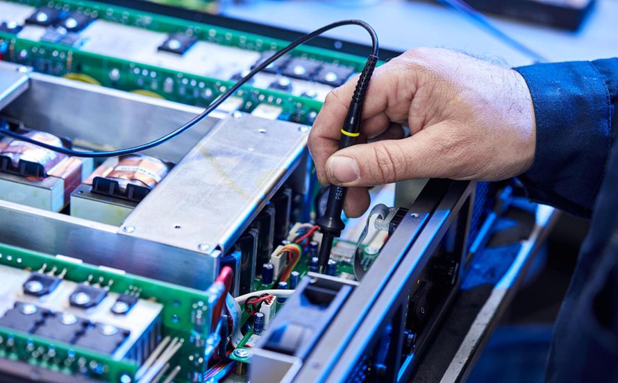
PCB Traceability and Labeling in Production Traceability is the ability to say, for any board in the field, which materials and which processes produced it. It is requested by customers in automotive, medical and industrial markets, and it is invaluable to the manufacturer, because a defect that can be traced…
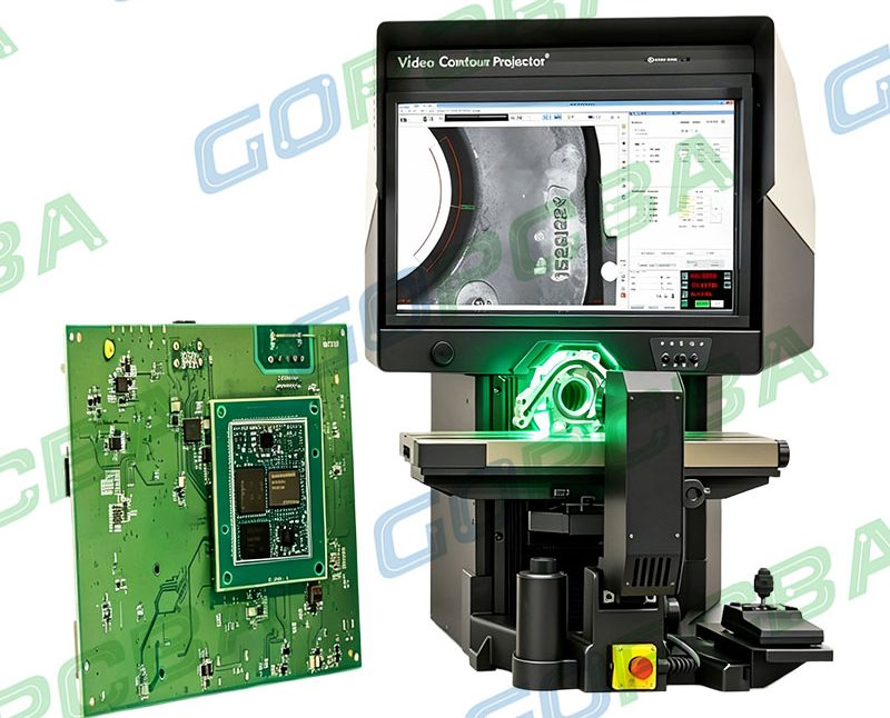
PCB Marking and Traceability Requirements Explained Every board carries some form of marking, whether it is a part number etched into the copper, a date code printed in the legend or a laser etched serial number on a panel. Marking looks like a trivial requirement until a field failure has…
Filament: Preparation, Placement and Process Control Conductive anodic filament growth is a failure that forms inside the laminate rather than on its surface. Copper migrates along the glass fibres under a voltage bias in the presence of moisture, and the filament that results grows until two conductors are connected. It…
Solder Preforms in Electronics Assembly Paste works because it can be printed everywhere at once and then melts into a joint. It fails when the joint needs more alloy than a stencil aperture can leave behind, when the surfaces are too massive for the heat the paste can carry, or…
Underfill Selection and Cure for Flip Chip and BGA Assemblies Solder joints under a large area array package are asked to survive thermal cycles that strain them in shear. The die and the substrate expand at different rates, and the outermost joints absorb most of the mismatch because they sit…
Bare Board Electrical Test Methods and Net Coverage A finished printed circuit board can look perfect and still be scrap. An open trace under a connector, a short between two nets hidden by the mask, or a plated hole that never made contact with an inner layer are all invisible…
Handling and Packaging of Finished PCBs: Best Practice A finished printed circuit board leaves the factory as a chemically active, moisture sensitive and static sensitive product, and the way it is packed decides whether it arrives in the condition it left in. Packaging is often treated as a shipping detail,…
Foreign Object and Debris Control in PCBA Assembly Foreign objects and debris cause failures that are difficult to explain because the object is usually gone by the time the failure is investigated. A metal fragment inside a housing, a solder ball in a connector or a stray fibre on a…
SMT Line Changeover: Program Recall, Feeder Setup and First Article A changeover replaces one product with another on the same line. The risk is not the new product, which is set up deliberately, but the remains of the old one, which are removed by assumption. Line Clearance Every component of…
Spray Coating: Selective Coating Methods Compared Selective coating applies protection where it is wanted and leaves the rest clear. The methods differ in how they build the film and in what they can reach, and the choice follows the board rather than the cost per board. Spray Coating A spray…