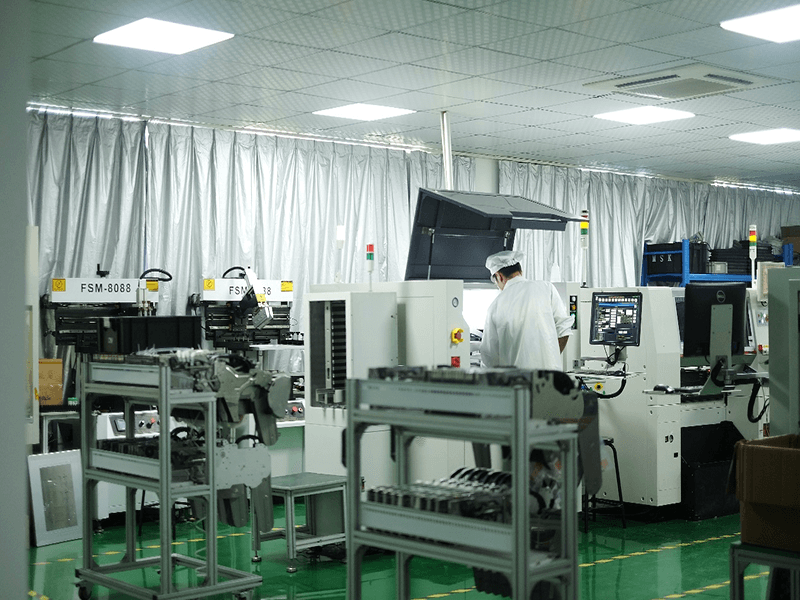
Solder Bead Prevention in Assembly A solder bead is a small sphere of solder that sits on the board surface away from any joint. Beads are usually between the size of a grain of sand and a pinhead, they are not part of the circuit, and they are a problem…
PCB Copper Plating Specification: Practical Process Controls Modern electronics depend on boards that are assembled correctly the first time. Every product – a phone, a charger, a medical instrument or an industrial controller – relies on thousands of solder joints that must conduct current for years. This article explains PCB…
PCB Copper Plating Sample: Practical Process Controls Modern electronics depend on boards that are assembled correctly the first time. Every product – a phone, a charger, a medical instrument or an industrial controller – relies on thousands of solder joints that must conduct current for years. This article explains PCB…
PCB Copper Plating Environment: Practical Process Controls Buyers and engineers often focus on the finished product and forget the production line behind it. In practice, most field failures can be traced back to process decisions made during assembly. Understanding PCB copper plating environment gives you a practical advantage when you…
PCB Copper Plating Handover: From Design to Repeatable Production Modern electronics depend on boards that are assembled correctly the first time. Every product – a phone, a charger, a medical instrument or an industrial controller – relies on thousands of solder joints that must conduct current for years. This article…
ICT Fixture Probe Selection for Assembled Board Testing In-circuit test still catches the faults that optical inspection cannot see: a wrong value, a reversed diode, a short under a shield, a connector pin that was never soldered. The inspection methods that cover the rest of the faults are set out…
Electroless Nickel Thickness Control On Copper Pads An electroless nickel immersion gold finish is built on a layer of nickel that is deposited without current and therefore covers every exposed copper surface evenly. That nickel layer is the structural part of the finish: it stops copper diffusing into the gold,…
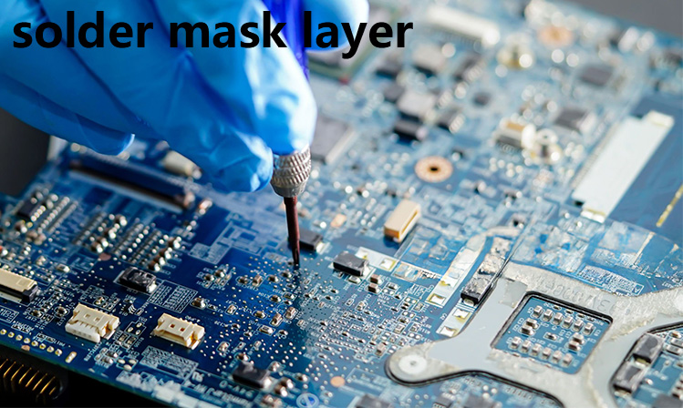
Solder Mask Thickness Selection For PCB Builds Solder mask thickness is rarely discussed until a board fails for a reason that traces back to it. The coating has to cover the copper, insulate adjacent features, protect the laminate during assembly and hold its shape around every pad and via. A…
PCB Copper Plating Risks: Design and Assembly Considerations Electronics manufacturing has become a discipline of small details. Solder paste volumes, placement accuracy, temperature profiles and inspection limits all add up to the final result. This guide looks at PCB copper plating risks from the perspective of a PCBA factory floor,…
PCB Copper Plating Review: Design and Assembly Considerations Buyers and engineers often focus on the finished product and forget the production line behind it. In practice, most field failures can be traced back to process decisions made during assembly. Understanding PCB copper plating review gives you a practical advantage when…