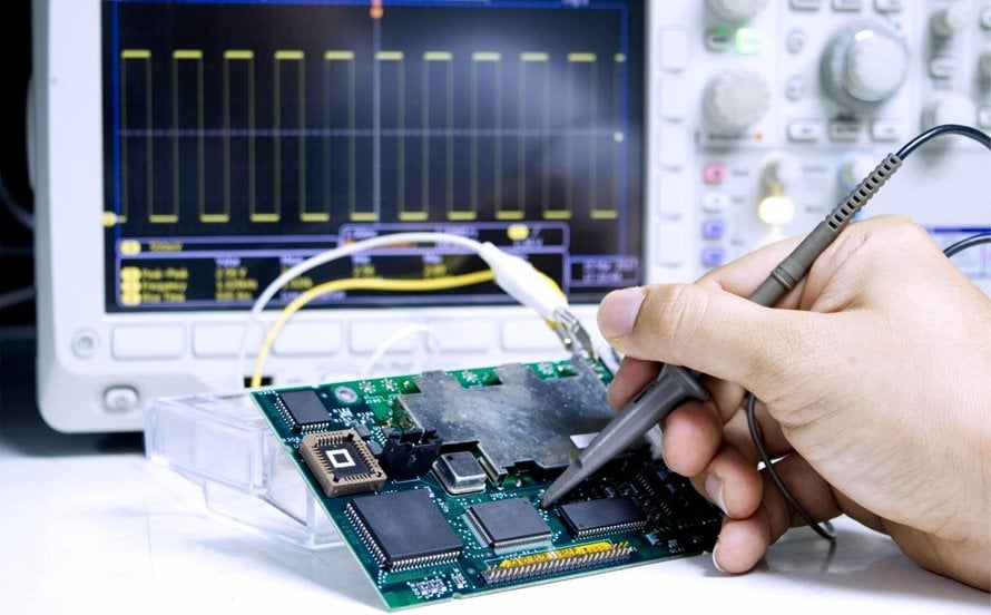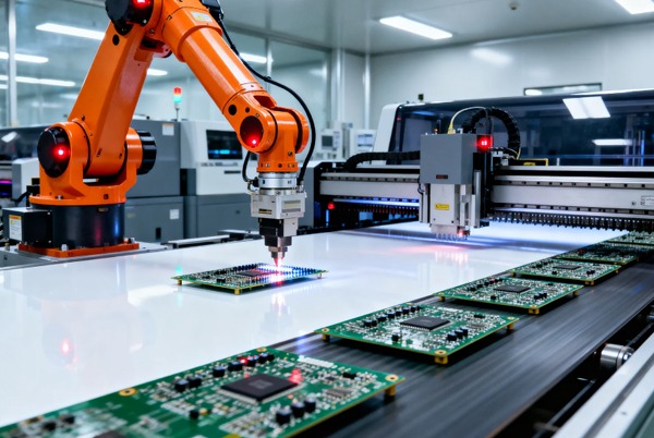
PCB Wave Solder Selection: A Practical Manufacturing Guide Buyers and engineers often focus on the finished product and forget the production line behind it. In practice, most field failures can be traced back to process decisions made during assembly. Understanding PCB wave solder selection gives you a practical advantage when…
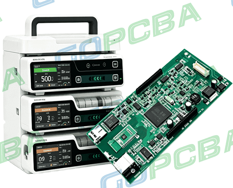
Solder Mask Dam Design Between Pads A solder mask dam is the strip of mask ink that runs between two adjacent pads. Its purpose is to stop molten solder from flowing from one land to the next, and its width is one of the few dimensions in a board design…
Board Handling and Scratch Prevention in PCB Assembly Most boards are damaged by the way they are moved rather than by the way they are made. A scratch across a solder mask, a chip on a panel edge, a fingerprint on a gold pad or a scuff on a finished…
Solder Balling Control In Reflow Soldering Solder balling is the scattering of small spherical solder particles around a joint after reflow. The balls range from a few micrometres to a few hundred micrometres across, they are usually attached only lightly to the surface, and they are a reliability problem because…
PCB Wave Solder Traceability: A Practical Review for Manufacturing Teams Modern electronics depend on boards that are assembled correctly the first time. Every product – a phone, a charger, a medical instrument or an industrial controller – relies on thousands of solder joints that must conduct current for years. This…
Low Temperature Solder Reflow Process Control for Assemblies Reducing the peak temperature of a reflow process sounds like a simple saving, but it changes the alloy, the flux, the joint appearance and the reliability of the finished product. Low temperature solder is used because thin boards warp, because some components…
PCB Wave Solder Improvement: A Factory-Floor Review Electronics manufacturing has become a discipline of small details. Solder paste volumes, placement accuracy, temperature profiles and inspection limits all add up to the final result. This guide looks at PCB wave solder improvement from the perspective of a PCBA factory floor, covering…
PCB Reflow Profile Limits: Key Process and Quality Checks Modern electronics depend on boards that are assembled correctly the first time. Every product – a phone, a charger, a medical instrument or an industrial controller – relies on thousands of solder joints that must conduct current for years. This article…
MCPCB Dielectric Thickness and Withstand Voltage The dielectric layer in a metal core PCB carries three jobs at once. It must isolate the circuit, conduct heat, and survive thermal cycling without cracking. Thickness is the variable that ties these jobs together, so it deserves a deliberate decision rather than a…
PCB Lead Time Planning Guide Lead time is the sum of the time a board spends being worked on and the time it spends waiting, and in most board shops the waiting is the larger part. A panel that takes four hours of actual processing can easily occupy ten working…