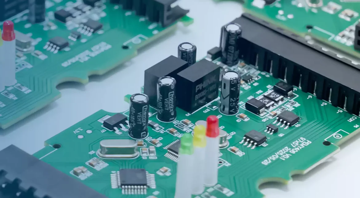
Reflow Self-Alignment and Placement Tolerance Limits Place a chip resistor half a pad width off centre and it often ends up perfectly centred after reflow. This is not luck; it is surface tension doing the work, and the industry has quietly relied on it for decades. Relying on it too…
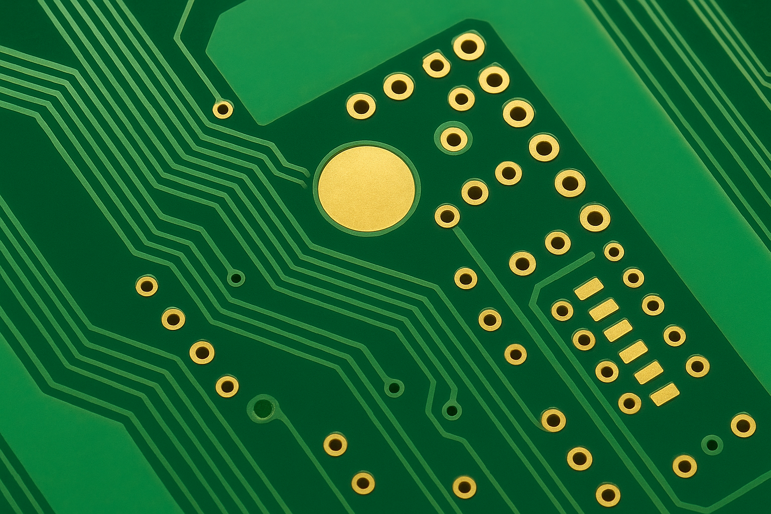
Solder Mask Design Rules: Dams, Slivers and Openings Solder mask is not decoration. It keeps solder where it belongs, protects the copper from the environment, and defines the resolution of a fine pitch layout. The rules that govern it are geometric and they collide with each other. What the Mask…
PCB Flux Activity Test: Process Details and Inspection Points Electronics manufacturing has become a discipline of small details. Solder paste volumes, placement accuracy, temperature profiles and inspection limits all add up to the final result. This guide looks at PCB flux activity test from the perspective of a PCBA factory…
PCB Surface Energy Test: A Practical Review for Manufacturing Teams Electronics manufacturing has become a discipline of small details. Solder paste volumes, placement accuracy, temperature profiles and inspection limits all add up to the final result. This guide looks at PCB surface energy test from the perspective of a PCBA…
Pad Cratering and Microcracks in Ball Grid Array Assemblies A solder joint can be perfectly formed and still fail, because the weakest link is often not the solder at all. When a ball grid array is loaded in bending, the copper pad and the resin beneath it can crack before…
PCB Paste Printing Defects: A Practical Review for Manufacturing Teams Electronics manufacturing has become a discipline of small details. Solder paste volumes, placement accuracy, temperature profiles and inspection limits all add up to the final result. This guide looks at PCB paste printing defects from the perspective of a PCBA…
High Speed PCB Design: Seven Rules That Pay Off High speed PCB design is less about a special technique than about a set of habits that reduce the number of times a board has to be redone. The seven rules below are the ones that experienced designers apply on every…
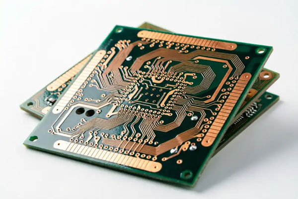
PCB Gold Finger Plating Thickness: Key Process and Quality Checks Buyers and engineers often focus on the finished product and forget the production line behind it. In practice, most field failures can be traced back to process decisions made during assembly. Understanding PCB gold finger plating thickness gives you a…
Seven Steps of PCB Design: From Library to Output A board that is designed twice costs twice as much, and most of the rework comes from skipping a step that takes an hour. The seven stages below are the ones that catch the mistakes while they are still cheap to…
PCB Drill Bit Wear and Its Effect on Plated Hole Quality A drill bit is a cutting tool that spends its life doing the hardest work in the fabrication shop. It wears progressively, and the wear shows up first in the quality of the hole wall rather than in the…