
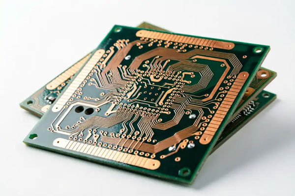
20 Layer PCB: Stackup, Design Rules and When It Pays What Twenty Layers Is For A 20 layer board is not simply a denser version of a 12 layer board. It exists because three problems appear together in high end systems and each of them consumes copper layers. High speed…
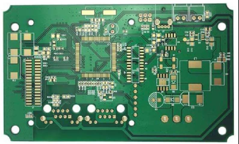
Embedded PCB vs Traditional PCB: How to Choose Two Different Answers to the Same Question A conventional board puts everything on the outside. The laminate carries the copper pattern, and the components, from a 0402 resistor to a large IC, are soldered to the surface. It has been the industry…
IPC Class 3 PCB: Requirements and Manufacturing Reality What Class 3 Actually Commits You To IPC classification runs from 1 to 3 and describes the consequence of failure rather than the difficulty of the build. Class 1 covers general electronics where the main requirement is that the product works. Class…
VIPPO PCB: Via-in-Pad Plated Over Explained What VIPPO Actually Means The acronym stands for via-in-pad plated over, and each part of the phrase describes a step. A via is placed inside a component pad rather than beside it. The hole is filled with solid copper by electroplating, not with resin.…
Microvia PCB: HDI Structures, Design Rules and Cost What Makes a Via a Microvia The definition is dimensional, not descriptive. A microvia is a small via formed by laser rather than mechanical drilling, and it connects one layer to the layer immediately below it. The recognised thresholds are a diameter…
Halogen Free PCB: Materials, Standards and Trade-offs Why the Halogen Content Is Specified at All Flame retardancy in a conventional laminate is achieved with brominated epoxy resin. Bromine is effective, cheap and well understood, and that combination made it the default for decades. The problem appears when the material burns…
Microwave PCB Materials: Choosing a Substrate Above 1 GHz Where the Material Becomes the Circuit Microwave boards cover roughly 1 to 30 GHz, and in that range the laminate is not a passive carrier. Its dielectric constant sets the impedance and the propagation velocity, its dissipation factor converts signal into…
PCB Etching Cost: What Drives the Price of Every Trace The Step That Defines the Circuit Etching is where the circuit stops being an image and becomes copper. After the pattern has been exposed and developed onto the resist, the etchant removes the copper that is not protected, and what…
Wireless Charging PCB Design, Lead Time and Cost A Board That Is Partly an Antenna A wireless charging board is unusual because part of it is not a circuit at all. The spiral coil that couples energy magnetically is etched into the same copper as the driver electronics, and its…
ENIG Surface Finish: Process, Thickness and Defects A Thin Stack That Decides Assembly Yield Bare copper oxidises, and an oxidised pad does not solder. The surface finish exists to keep the copper clean until the assembly line reaches it, and to do so without changing the shape of the pad.…