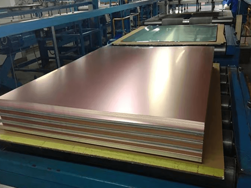
Developer pH Control: 5 Checks for Consistent Development Developer pH control is the parameter that keeps resist development repeatable from the first panel of a shift to the last. Alkaline developers lose strength as they dissolve resist, and the change is gradual enough that nobody notices until openings start to…
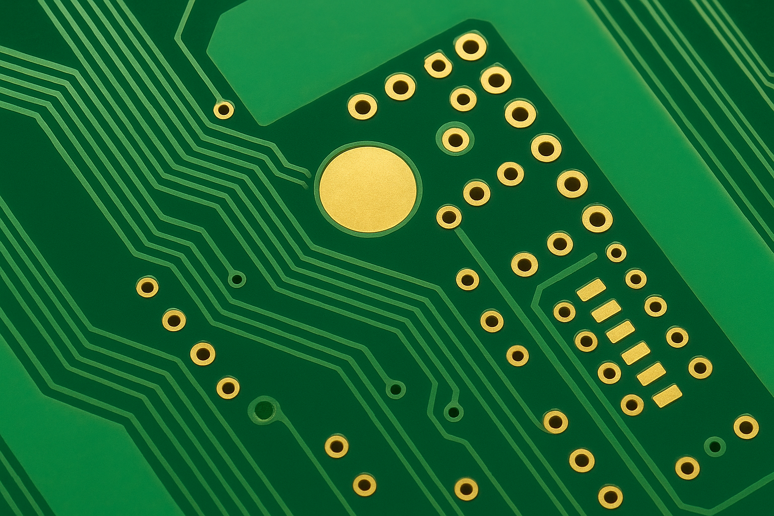
Lamination Vacuum Hold Time: 5 Settings for Void-Free Pressing Lamination vacuum hold time is the window during which air and volatiles can still leave the stack. Once the resin gels, anything trapped inside stays there as a void. The hold time therefore has to start early enough to remove air…
Exposure Lamp Life Management: 6 Rules for Consistent Imaging Exposure lamp life is managed by hours in most shops and by luck in the rest. Lamps do not fail; they fade. Output falls gradually, the operator compensates with exposure time, and the process drifts away from the window it was…
Step Tablet Exposure Test: 5 Rules for Reliable Dose Readings A step tablet exposure test converts an invisible lamp condition into a number that can be recorded, compared and acted on. Without it, exposure control depends on how the last panels looked, which is exactly how imaging processes drift quietly…
Press Cooling Under Pressure: 5 Steps for Stable Laminates Press cooling under pressure is the part of the lamination cycle that most shops treat as waiting time. Resin is still mobile while the stack is warm, and the way it cools decides how much the panel shrinks, how evenly it…
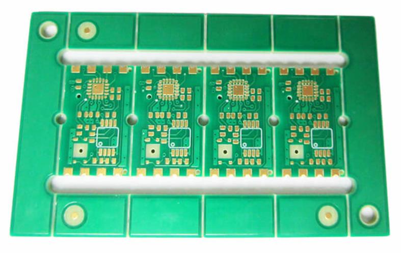
PCB Panel Size Sample: Process Details and Inspection Points Modern electronics depend on boards that are assembled correctly the first time. Every product – a phone, a charger, a medical instrument or an industrial controller – relies on thousands of solder joints that must conduct current for years. This article…
PCB Panel Size Plan: What Matters on the Production Line Modern electronics depend on boards that are assembled correctly the first time. Every product – a phone, a charger, a medical instrument or an industrial controller – relies on thousands of solder joints that must conduct current for years. This…
PCB Panel Size Risks: What Could Go Wrong Electronics manufacturing has become a discipline of small details. Solder paste volumes, placement accuracy, temperature profiles and inspection limits all add up to the final result. This guide looks at PCB panel size risks from the perspective of a PCBA factory floor,…
UV Exposure Energy Control: 5 Checks for Sharp Resist Images UV exposure energy is the dose that converts a photoresist pattern from artwork into a latent image, and it is usually the last variable an operator thinks to question. Exposure looks binary: the panel goes in, the lamps run, the…
PCB Panel Size Limits: From Prototype to Volume Production Electronics manufacturing has become a discipline of small details. Solder paste volumes, placement accuracy, temperature profiles and inspection limits all add up to the final result. This guide looks at PCB panel size limits from the perspective of a PCBA factory…