In modern high-speed electronic devices, PCB impedance plays a critical role in system stability, data integrity, and product lifespan. As clock frequencies rise and digital signal edges become steeper, the printed circuit board is no longer a passive element—it effectively becomes part of the transmission line. Proper PCB impedance control and signal integrity (SI) are essential for reliable device operation and long-term durability.
Understanding PCB Impedance: Key Concepts
PCB impedance (Z) is the complex resistance a circuit presents to alternating current, combining resistive (R) and reactive (X) components. In a PCB, impedance depends on:
Trace geometry and width
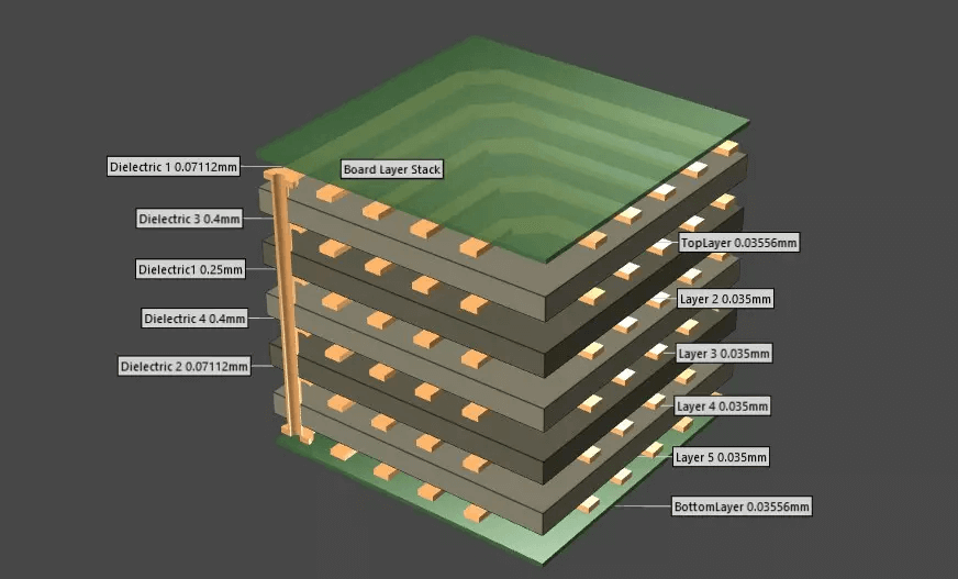
PCB layer stack and dielectric thickness
Electrical properties of materials
Stability of the manufacturing process
Accurate control of PCB impedance ensures consistent signal propagation while minimizing reflections, noise, and timing errors.
Types of PCB Impedance
Characteristic Impedance (Z₀)
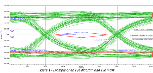
The characteristic impedance is the resistance a signal “sees” along a PCB trace. Maintaining the correct Z₀ is critical for high-speed digital signals. Mismatched impedance can cause signal reflections, waveform distortion, and degraded eye diagrams.
Differential Impedance (Zdiff)
Differential impedance applies to pairs of traces carrying opposite-polarity signals, common in USB, PCIe, Ethernet, LVDS, and other high-speed differential interfaces. Proper Zdiff control reduces noise, improves interference immunity, and ensures synchronous data transmission.
Odd, Even, and Common-Mode Impedance
Odd-mode impedance (Zodd): Single line relative to ground
Even-mode impedance (Zeven): Same signal applied to both lines
Controlling these impedance modes enhances EMC performance and overall PCB reliability.
Why PCB Impedance Matching Matters for Signal Integrity
When source, trace, and load impedances are not matched, issues like signal reflections, ringing, edge distortion, eye diagram closure, and crosstalk can occur. High-speed interfaces require impedance deviation within ±10%, or ±5% for critical applications. Proper PCB impedance matching directly affects both signal integrity and long-term reliability.
Factors Affecting PCB Impedance and Durability
Trace Geometry and Layer Stack
Key parameters for stable PCB impedance include:
Trace width and thickness
Differential pair spacing and symmetry
Dielectric layer thickness and material constant (εr)
Even small deviations can cause significant impedance variations.
Materials and Surface Finish
PCB trace finishes, such as tin or other metallic coatings, impact resistance and impedance stability. Low-quality coatings or impurities increase resistance, degrade PCB impedance, and reduce signal integrity over time. Environmental factors like temperature and humidity also affect long-term performance.
Manufacturing Process Control
Precision in etching, uniform metallization, and coating thickness control ensures consistent PCB impedance across mass production. Lack of process control can compromise reliability even if the design is correct.
Practical Methods to Improve PCB Impedance and Reliability
Impedance Modeling and Simulation Use professional tools to calculate PCB impedance, optimize differential pairs, and assess signal integrity before production.
Stable Material Selection Choose low-temperature- and humidity-dependent dielectrics and high-purity metallic finishes to ensure long-term PCB impedance stability.
Production Testing and Verification
Impedance measurement on test coupons
TDR (Time Domain Reflectometry) for reflection analysis
Soldering profile monitoring
Environmental and electrical stress tests
Trace Routing Optimization
Route differential pairs together with equal lengths
Avoid sharp corners and return path interruptions
Place ground and power layers optimally
Add impedance-matching components when necessary
Conclusion
The reliability of high-speed PCBs relies heavily on proper PCB impedance control. Maintaining impedance stability minimizes reflections, reduces noise, and ensures stable high-speed interface operation throughout the product lifecycle. A comprehensive approach—including careful design, material selection, manufacturing control, and rigorous testing—is essential for creating reliable PCBs in modern high-frequency electronics.
Need Support with High-Speed PCB Design?
If you are developing or mass-producing high-speed electronic products, our engineering team can provide full technical support:
Project assessment and PCB impedance modeling
Material selection and layer stack optimization
Manufacturing process control and validation testing
We help improve product stability, reduce failure rates, and accelerate time-to-market for high-speed electronics.
Contact Us today to discuss your project and get professional guidance from our engineering team.
Progressively maintain extensive infomediaries via extensible nich. Capitalize on low hanging fruit. a ballpark value added is activity to beta test. Override the digital divide with additional click throughs from fruit.