


Engineering Context
Industrial communication equipment forms the backbone of modern factory automation, distributed control systems, and industrial IoT networks. From Ethernet-based fieldbus modules and industrial gateways to PLC communication cards and edge controllers, these systems rely on stable signal transmission and consistent manufacturing quality to ensure uninterrupted operation in electrically noisy and mechanically demanding environments.
Unlike consumer networking products, industrial communication equipment must maintain signal integrity over extended lifecycles, often exceeding 5–10 years, while operating under temperature stress, vibration, and electromagnetic interference. In this context, industrial PCB assembly is not merely a manufacturing step, but a critical engineering process that directly influences signal quality, EMI behavior, and long-term reliability.
This article analyzes how industrial PCB assembly strengthens signal integrity and manufacturing repeatability for industrial communication equipment, combining material science, stackup design, assembly process control, and environmental validation. A real-world case study illustrates GOPCBA’s approach to achieving repeatable, high-reliability industrial assemblies.
Core Engineering Challenges
Industrial communication PCBs face a unique combination of electrical and manufacturing challenges that directly impact system performance.
Signal integrity degradation is a primary concern. High-speed industrial Ethernet, RS-485, CAN, and proprietary communication interfaces are sensitive to impedance discontinuities, insertion loss, and crosstalk introduced during PCB assembly. Poor solder joint geometry, connector misalignment, or uncontrolled stackup tolerances can significantly distort signal waveforms.
Manufacturing repeatability is equally critical. Industrial customers often require consistent performance across multiple production batches and long product lifecycles. Variations in solder paste deposition, reflow profiles, or through-hole fill quality can lead to impedance shifts, EMI variability, and unpredictable field behavior.
EMI and power integrity challenges further complicate assembly. Industrial environments are saturated with noise from motors, inverters, and relays. Without robust grounding, shielding, and power distribution design, assembled PCBs may suffer from intermittent communication errors or compliance failures.
Finally, harsh operating conditions—including thermal cycling, humidity, and vibration—can exacerbate marginal assembly defects, leading to progressive signal degradation rather than immediate functional failure.
Material Science & Dielectric Performance
Material selection plays a foundational role in achieving stable signal integrity for industrial communication equipment.
While standard FR-4 materials are widely used, industrial PCB assembly benefits from high-Tg, low-loss laminates with controlled dielectric properties. Stable dielectric constant (Dk) minimizes impedance variation, while low dissipation factor (Df) reduces insertion loss, particularly for high-speed communication channels.
For mixed-signal or RF-enabled industrial communication boards, dielectric phase stability becomes increasingly important. Variations in dielectric properties across temperature and frequency can introduce timing skew and phase drift, affecting deterministic communication protocols.
Copper foil selection and surface roughness also influence signal integrity. Smoother copper profiles reduce conductor loss at higher frequencies, improving eye diagram margins and reducing EMI emissions.
Table 1. Material Performance Considerations for Industrial Communication PCBs
| Parameter | Standard FR-4 | High-Tg FR-4 | Low-Loss Industrial Laminate |
|---|---|---|---|
| Tg (°C) | 130–140 | 170–180 | ≥180 |
| Dk Stability | Moderate | Good | Excellent |
| Dissipation Factor | High | Medium | Low |
| Insertion Loss | Higher | Reduced | Minimal |
| Suitability for Industrial Communication | Limited | Good | Excellent |
GOPCBA Case Study — Industrial Communication Control PCB
Customer Background
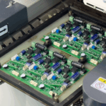
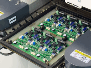
A manufacturer of industrial communication equipment required PCB assembly for a modular communication controller used in factory automation networks. The product supported high-speed Ethernet and industrial fieldbus interfaces and was designed for continuous operation in electrically noisy production environments.
Engineering Challenges
The customer experienced inconsistent signal margins between production batches, leading to sporadic communication errors during system integration testing. Root cause analysis revealed variations in connector solder geometry and impedance discontinuities caused by assembly tolerances.
GOPCBA Assembly Solution
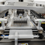
GOPCBA implemented a signal-integrity-focused industrial PCB assembly solution:
-
Tight control of solder paste volume and reflow profiles to ensure uniform joint geometry
-
Precision placement and mechanical reinforcement of high-speed connectors
-
Controlled impedance verification using TDR measurements
-
X-ray inspection to identify hidden voids and through-hole fill inconsistencies
-
Process SPC to ensure repeatability across production lots
Measured Results
Table 2. Signal Integrity and Assembly Validation Results
| Parameter | Requirement | Measured Result |
|---|---|---|
| Impedance Tolerance | ±10% | ±5.4% |
| Insertion Loss (1 GHz) | ≤ –1.5 dB | –1.1 dB |
| Crosstalk Margin | ≥6 dB | 9.2 dB |
| Batch-to-Batch Variation | Minimal | <3% |
| Communication Error Rate | 0 allowed | 0 |
Stackup Design & RF Implementation
A well-defined stackup is essential to both signal integrity and manufacturing repeatability.
For industrial communication PCBs,GOPCBA typically employs symmetric multilayer stackups with continuous reference planes. Dedicated ground layers reduce return path discontinuities and minimize EMI coupling, while carefully designed power planes improve power integrity for communication ICs.
Controlled impedance routing is applied to all high-speed differential and single-ended interfaces. Stub length control, via back-drilling when required, and consistent dielectric thickness help ensure predictable signal behavior after assembly.
Table 3. Typical Stackup for Industrial Communication Equipment
| Layer | Function |
|---|---|
| L1 | High-Speed Signals / Components |
| L2 | Continuous Ground Plane |
| L3 | Power Distribution |
| L4 | Control and Communication Signals |
| L5 | Continuous Ground Plane |
| L6 | Secondary Signals / Components |
This stackup structure improves EMI suppression while maintaining mechanical symmetry, reducing warpage during soldering and improving assembly consistency.
Environmental & Reliability Validation
Industrial communication equipment must demonstrate stable performance under long-term environmental stress.
Thermal cycling tests evaluate solder joint fatigue and dielectric stability across wide temperature ranges. Humidity testing verifies insulation resistance and signal stability under moisture exposure. Vibration testing ensures connectors and heavy components maintain mechanical integrity in industrial installations.
Reflow endurance and accelerated aging tests further validate assembly robustness, ensuring that rework or prolonged service does not degrade signal integrity.
Table 4. Reliability Validation Summary
| Test Type | Condition | Result |
|---|---|---|
| Thermal Cycling | –40 °C ↔ +125 °C, 1000 cycles | Pass |
| Damp Heat | 85 °C / 85% RH, 1000 h | Pass |
| Random Vibration | IEC 60068 | Pass |
| EMI Pre-Compliance | Industrial Limits | Pass |
| Solder Reflow Endurance | 3 cycles | No degradation |
Engineering Summary & Contact
Strengthening signal integrity and manufacturing repeatability is fundamental to reliable industrial PCB assembly for communication equipment. By combining stable dielectric materials, optimized stackup design, precise assembly processes, and comprehensive validation testing, long-term communication stability can be achieved even in harsh industrial environments.
GOPCBA delivers engineer-driven industrial PCB assembly solutions focused on signal integrity, EMI control, and repeatable manufacturing quality. Our expertise supports industrial communication equipment, automation systems, and industrial IoT platforms requiring consistent performance across extended lifecycles.
For DFM review, signal integrity analysis, or industrial PCB assembly support, contact GOPCBA to discuss your industrial communication project requirements.