10 Layer Any Layer HDI PCB: Advanced High Density Interconnect Technology for High Performance Electronics
With the continuous development of electronic products toward miniaturization, higher performance, and greater functionality, PCB technology faces increasingly demanding challenges. The 10 Layer Any Layer HDI PCB has become a key solution for next-generation electronic devices due to its excellent signal integrity, high-density interconnection capability, and advanced manufacturing technology.
Compared with conventional multilayer circuit boards, any-layer HDI technology provides greater wiring flexibility and improved electrical performance. It enables complex electronic systems to achieve higher integration levels while maintaining reliable signal transmission.
For applications requiring advanced circuit structures, professional HDI PCB Manufacturing capabilities are essential to ensure precision control, stable production quality, and reliable performance.
The structure of a 10 Layer Any Layer HDI PCB is designed with advanced interconnection technology to meet the requirements of modern high-performance electronics.
The 10-layer stack-up provides sufficient space for signal routing, power distribution, and grounding design. Through any-layer microvia interconnection technology, each layer can be directly connected without being limited by traditional through-hole structures.
Unlike conventional PCBs that rely heavily on mechanical vias, any-layer HDI boards utilize laser-drilled microvias and blind vias to shorten signal paths. This helps reduce signal transmission delays, minimize signal reflection, and improve high-frequency performance.
The optimized structure provides several advantages:
These characteristics make 10-layer any-layer HDI boards ideal for advanced products requiring compact design and powerful processing capabilities.
Material selection plays a critical role in the performance and reliability of a Multilayer PCB.
For high-speed and high-frequency applications, manufacturers often select advanced low-loss materials such as Rogers RO4350B and Panasonic Megtron 6. These materials provide stable dielectric properties and low dissipation factors, helping reduce signal loss and improve transmission efficiency.
Typical material advantages include:
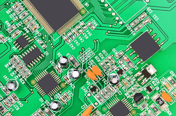
In addition to substrate materials, copper foil selection is also important. Reverse-treated copper foil with lower surface roughness can reduce insertion loss and signal reflection, improving high-frequency signal performance.
For applications with demanding thermal requirements, special materials with enhanced heat dissipation capability may also be integrated to improve long-term reliability.
Professional PCB Capabilities ensure manufacturers can handle advanced materials, complex stack-ups, and precision fabrication requirements for high-layer-count HDI boards.
Producing a 10 Layer Any Layer HDI PCB requires advanced manufacturing technology and strict process control. Each manufacturing stage directly affects electrical performance and product reliability.
Multi-layer lamination is one of the most challenging processes in HDI PCB manufacturing.
During the lamination process, ten layers of materials must be precisely aligned and bonded together. Even a small alignment error may affect via connections, signal performance, and overall reliability.
Advanced positioning systems and high-precision lamination equipment are used to ensure accurate layer registration. Under controlled temperature and pressure conditions, multiple layers are combined into a stable and reliable PCB structure.
Laser drilling is a core technology used in HDI PCB Manufacturing.
Compared with traditional mechanical drilling, laser drilling can create extremely small microvias, allowing more compact routing designs and higher circuit density.
After microvia formation, copper filling technology is applied to create reliable electrical connections between layers. The plating process requires precise control of current density, chemical concentration, and process parameters to ensure uniform copper coverage.
High-quality via filling prevents problems such as:
The circuit formation process uses advanced imaging technology to transfer designed circuit patterns onto the PCB surface.
During etching, unnecessary copper is removed through controlled chemical processes to create accurate traces.
Important parameters such as etching speed, solution concentration, and temperature must be carefully controlled to maintain:
This precision is especially important for high-density HDI boards with fine-pitch routing requirements.
Surface treatment improves solderability, corrosion resistance, and long-term reliability.
Common surface finishes include:
ENIG provides excellent soldering performance and stable electrical contact. The gold layer protects copper surfaces from oxidation and improves connection reliability.
Hard gold is suitable for areas requiring high wear resistance and frequent electrical contact.
OSP forms a protective coating on copper surfaces, preventing oxidation while maintaining good soldering performance.
Quality inspection is a critical stage in producing reliable PCB Manufacturing products.
Advanced inspection equipment is used to evaluate appearance, dimensions, electrical performance, and manufacturing consistency.
High-resolution optical inspection systems check PCB surfaces for:
Dimensional testing verifies:
These inspections ensure the PCB meets design specifications and can be successfully integrated into final electronic systems.
For applications requiring complete assembly verification, professional PCBA Testing services provide additional reliability assurance through electrical testing and functional validation.
The excellent performance of the 10 Layer Any Layer HDI PCB makes it widely used across multiple advanced industries.
In 5G base stations and premium smartphones, high-density HDI technology supports complex RF circuits, processors, and communication modules.
Its excellent signal transmission capability helps achieve:
AI servers, data centers, and advanced computing systems require extremely high-speed data processing capabilities.
The superior electrical performance of 10-layer any-layer HDI boards helps improve system stability and processing efficiency.
Aerospace applications require PCBs that can operate reliably under extreme conditions such as temperature changes, vibration, and radiation exposure.
The high reliability and stable performance of HDI technology make it suitable for avionics systems, satellite communication equipment, and other mission-critical electronics.
As electronic products continue evolving toward higher integration, smaller size, and faster performance, the demand for advanced HDI solutions will continue to grow.
The 10 Layer Any Layer HDI PCB represents an important direction in modern PCB development by combining high-density routing, excellent signal integrity, and advanced manufacturing technology.
Through continuous innovation in materials, process optimization, and quality control, professional PCB manufacturers can provide reliable solutions for industries including telecommunications, artificial intelligence, industrial electronics, medical equipment, and aerospace.
By selecting an experienced manufacturing partner with strong engineering capabilities and advanced production technology, companies can achieve higher product performance, shorter development cycles, and improved market competitiveness.