10-Layer 1.6mm Controlled Impedance PCB Guide
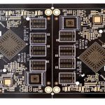
A ten-layer board at 1.6mm finished thickness gives high-speed designs room for dedicated signal, power and ground layers. Controlled impedance ties that stack-up to predictable transmission-line behavior. The combination suits networking gear, optical modules, radar units and dense computing boards. This guide explains the decisions that matter before fabrication starts. It covers stack-up planning, trace geometry, via structures, lamination control and the inspection steps a buyer should confirm.
Board thickness alone tells you little about electrical performance. What matters is how the copper, prepreg and core layers are arranged, and how each signal layer references a plane. A 1.6mm build is common because it balances rigidity, connector fit and routing capacity. Engineers should treat the stack-up as a design input, not a fabrication afterthought. The final arrangement should follow the target impedance, copper weight, dielectric properties and routing density of the actual design.
Stackup Planning Basics
Ten conductive layers let the designer separate high-speed signals from noisy power switching. A typical arrangement places signal layers next to ground planes so return currents stay short. Power planes sit in the middle, often in pairs, to add distributed capacitance and lower plane impedance. Symmetry matters for warpage control during lamination and reflow. An unbalanced build may pass electrical test and still bow in the assembly oven. Review the layer assignment with the fabricator before releasing artwork.
Dielectric thickness between a signal layer and its reference plane sets the impedance more than any other single variable. Small changes in prepreg thickness shift impedance noticeably on fine traces. The fabricator should confirm which prepreg constructions are available and how they behave after pressing. Ask for the as-built stack-up, not just the nominal one. Buyers reviewing a quote should also check that the impedance targets match the connector and cable specifications. A mismatch at the interface causes reflections that no amount of tuning inside the board can fix.
Trace Width and Spacing
Fine-line capability around 3/3 mil is common in advanced shops, but the design should not use it without reason. Narrower traces raise resistive loss and demand tighter etching control. Wider traces ease fabrication and improve current capacity. The right width comes from the impedance target, the dielectric height and the copper thickness, calculated together. Spacing between traces controls crosstalk, especially on parallel high-speed buses. Designers should verify both values against the fabricator capability before layout freeze.
Etching is not perfectly vertical, so the finished trace is narrower at the top than at the base. Fabricators compensate in the artwork, but the compensation depends on copper weight and line width. Very fine lines are more sensitive to this effect. A design that pushes the process limit leaves little margin for normal variation. Engineers should ask what tolerance the shop holds on trace width and how it verifies that value.
Good PCB design and layout practice keeps critical traces inside proven capability rather than at the edge of it.

Impedance Control Targets
Controlled impedance means the fabricated transmission line lands inside a specified window. A common tolerance is plus or minus ten percent, and tighter windows are possible on selected designs. The target applies to single-ended traces and to differential pairs, each with its own geometry. Impedance depends on trace width, dielectric thickness, dielectric constant and copper thickness. None of these is fixed in production, so the window must absorb normal process drift. The fabricator should state how it measures and reports the result.
Test coupons built alongside the panel give the clearest evidence. Time-domain reflectometry on those coupons shows whether the lines meet the target. Coupons should be designed with the same geometry as the functional traces. A coupon that does not represent the real routing proves little. Ask whether the report includes per-layer data or only a summary. Buyers comparing suppliers should treat impedance data as a routine deliverable, not a special request. It belongs with the quality management records for every lot.
Via Structures and Drilling
High-density layouts often need small vias, including laser-drilled microvias and mechanical blind vias. These structures free routing space around fine-pitch packages. They also add process steps and cost. Every via transition disturbs the transmission line, so via count on critical nets should stay low. Stub length on through vias matters at high data rates. Back drilling can remove unused stub, but it adds cost and needs planning. The stack-up should show which via types are allowed on which layers.
Laser drilling quality depends on material, energy, depth control and positioning accuracy. The subsequent metallization must fill and plate the via reliably. Aspect ratio limits how deep a small via can go, so the fabricator should confirm what the design requires. Pad size and annular ring must survive registration tolerance. Ask for cross sections showing via shape and plating thickness. A supplier that cannot show this data is asking you to trust an unverified process. Rapid PCBA prototyping is a sensible place to prove these structures before volume.
Lamination and Registration
Ten layers means many pressing cycles and many chances for misregistration. The inner layers must align to each other and to the drill program. Lamination needs the right resin flow, heating rate, pressure and cooling profile. Poor control shows up as voids, delamination, resin starvation or excessive warp. For impedance-controlled designs, lamination also sets the final dielectric thickness. A press that runs slightly thin shifts every impedance value on that layer pair. Process records should include the press profile used for the lot.
Material choice interacts with lamination. Higher-performance laminates may need different press cycles than standard FR-4. Mixing material types in one stack-up is possible but needs care at the interfaces. Buyers should confirm that the fabricator has qualified the specific combination, not just each material separately. Component procurement and material sourcing should be planned together so the laminate and the parts arrive in time for the build. Late material changes are a common cause of impedance drift between lots.
Inspection and Test Coverage
Optical inspection catches opens, shorts, missing features and pattern defects on inner and outer layers. Electrical test verifies continuity and isolation across the whole netlist. Neither step proves impedance, so coupon measurement is needed as well. Cross sections confirm dielectric thickness, plating quality and via shape. Dimensional checks confirm board outline, hole position and thickness. Together these checks cover most failure modes on a ten-layer build. The inspection plan should name each check and the sampling rate.
Test coverage should match the risk of the design. A dense high-speed board with fine lines and microvias deserves more sampling than a simple control board. Ask how the fabricator handles a lot that fails impedance on one coupon. Does it re-measure, adjust, or scrap? The answer shows whether the process is understood or merely inspected. Buyers should also confirm that the same checks run on repeat orders. A first article that passes and a second lot that skips the coupons is a quality gap waiting to surface.
Buyer Verification Checklist
Before release, confirm the as-built stack-up, the impedance targets and the measurement method. Check that trace width and spacing sit inside proven capability. Review the via types and the cross-section data from a similar build. Ask for the lamination profile and the material certificates. Confirm the inspection plan and the sampling rates. Finally, agree what happens when a result falls outside the window. Written answers to these questions turn a quotation into a plan. They also give the assembly team a stable board to build on.
Volume production adds one more concern: consistency across lots. Parameters drift, materials change and operators rotate. A supplier that records process data and reviews trends will catch drift early. A supplier that relies on final inspection alone will find problems after the boards are built. For high-speed designs, that difference shows up as yield loss and field returns. High-volume PCB assembly works best when the bare board supplier and the assembler share the same stack-up and inspection records.
The practical takeaway is simple. Treat the 1.6mm ten-layer stack-up as an engineered system with measured outputs. Agree the impedance targets, the coupon method and the reporting format before tooling. Keep fine lines and small vias inside qualified capability. Require cross sections and lot records with every shipment. Taking these steps early is inexpensive and helps avoid costly problems later on. A board that meets its impedance window on the first lot and the tenth is worth more than a lower quote with no data behind it.