10 PCB DFM Optimization Tips to Reduce PCB Manufacturing Costs
In the PCB manufacturing process, PCB DFM optimization plays a critical role in controlling production costs and improving manufacturing efficiency. Proper Design for Manufacturability (DFM) adjustments can reduce material waste, simplify production processes, improve yield rates, and significantly lower overall manufacturing expenses without sacrificing product performance.
For companies looking to develop reliable and cost-effective electronic products, optimizing PCB design at the early stage is one of the most effective ways to achieve long-term cost savings.
This article introduces 10 proven DFM optimization techniques that help engineers create more manufacturable PCB designs while maintaining electrical performance and reliability.
1. Optimize PCB Edge Design and Board Dimensions
PCB edge design and overall board dimensions directly affect material utilization during manufacturing.
Whenever possible, designers should use simple geometric shapes, such as rectangular boards, instead of complicated irregular shapes. Non-standard PCB shapes often create additional material waste during cutting and may require special fixtures or customized tooling, increasing both production time and manufacturing costs.
Another effective approach is optimizing panel utilization. By combining multiple small PCB designs into a standard manufacturing panel size, manufacturers can maximize material usage and reduce unnecessary waste.
Improving panel efficiency can directly reduce material consumption and lower the total cost of PCB manufacturing.
Working with experienced manufacturers through professional PCB fabrication services can help engineers optimize board dimensions according to actual production capabilities.
2. Select the Right PCB Material Specifications
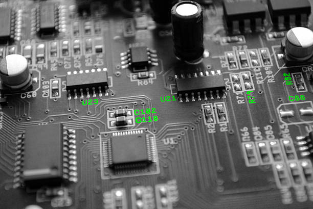
PCB material selection has a significant impact on manufacturing cost.
Different materials have different price levels, and selecting expensive materials without actual performance requirements can unnecessarily increase production expenses.
For applications that do not require extreme temperature resistance, high-frequency performance, or special environmental durability, standard materials such as FR-4 are often sufficient.
Using specialized high-frequency or high-speed materials should only be considered when required by electrical performance.
Additionally, designers should avoid selecting unnecessarily thick boards. If the required mechanical strength and electrical characteristics can be achieved with thinner materials, choosing a thinner PCB can reduce:
- Material cost
- Processing difficulty
- Manufacturing energy consumption
Proper material selection is an important part of effective PCB cost reduction.
3. Simplify PCB Layer Count
The number of PCB layers is one of the major factors influencing manufacturing cost.
Each additional layer increases production complexity, including:
- Lamination processes
- Drilling operations
- Inner-layer processing
- Inspection requirements
Therefore, reducing unnecessary layers can significantly decrease production expenses.
However, reducing layer count should not compromise electrical performance. Engineers need to balance cost, signal integrity, power requirements, and routing complexity.
By optimizing component placement and improving routing strategies, many designs can achieve lower layer counts while maintaining reliable performance.
For complex electronic applications, professional PCB design for manufacturing analysis can help determine the most cost-effective layer structure.
4. Optimize Via Size and Hole Distribution
PCB drilling is another important factor affecting manufacturing costs.
Smaller holes require higher precision equipment, longer drilling time, and stricter process control, which increases production costs.
Whenever possible, designers should use standard hole sizes instead of extremely small vias or customized drilling specifications.
Optimizing hole distribution is also important. Excessively dense or uneven hole placement may increase:
- Drill breakage risks
- Manufacturing difficulties
- Production defects
A well-planned hole layout improves manufacturing efficiency and reduces unnecessary production losses.
5. Standardize Copper Trace Width and Spacing
Copper trace width and spacing must meet electrical requirements, but excessive miniaturization can increase manufacturing difficulty and cost.
Using extremely fine traces may require:
- Advanced etching processes
- Higher inspection requirements
- More precise manufacturing control
When standard specifications are sufficient, designers should avoid unnecessary fine-line designs.
Using standard copper widths and spacing improves manufacturing yield, reduces processing complexity, and lowers production costs.
For advanced applications requiring high-density routing, engineers can work with professional PCB manufacturers to find a balance between performance and cost.
6. Reduce Unnecessary Special Surface Finishes
Different PCB surface finishes have significant cost differences.
Some advanced surface treatments provide excellent performance but may increase manufacturing expenses considerably.
When selecting surface finishes, designers should consider actual product requirements, including:
- Operating environment
- Product lifespan
- Electrical requirements
- Assembly requirements
If standard surface treatments can meet performance requirements, they are usually more cost-effective.
For designs requiring special surface finishes in specific areas, partial treatment may be considered instead of applying expensive processes across the entire PCB.
This approach can reduce surface treatment costs while maintaining required performance.
7. Optimize Solder Mask Design
Solder mask design also affects PCB manufacturing efficiency.
Complex solder mask openings and extremely small openings increase production difficulty because they require more precise exposure and development processes.
Common problems caused by complicated solder mask designs include:
- Higher manufacturing time
- Increased defect rates
- Additional processing costs
Using standard opening shapes, such as simple circular or rectangular designs, can simplify production and improve manufacturing consistency.
A well-optimized solder mask design helps reduce production risks and supports better PCB fabrication services.
8. Standardize Component Package Specifications
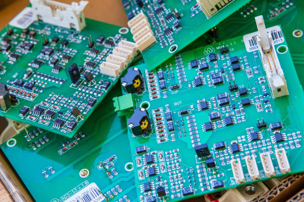
Inconsistent component packages can increase manufacturing complexity.
When a PCB contains many different package sizes for similar components, manufacturers may need to frequently adjust equipment settings, reducing production efficiency.
Standardizing component packages can provide several benefits:
- Faster assembly processes
- Reduced machine adjustment time
- Lower risk of assembly errors
- Improved production consistency
During the design stage, engineers should select commonly used component packages whenever possible instead of using multiple unnecessary package variations.
This approach improves manufacturing efficiency and contributes to overall PCB cost reduction.
9. Consider Production Volume and Process Compatibility
DFM optimization should always consider future production requirements and manufacturing processes.
For high-volume production, designs should prioritize processes that support automation and stable mass manufacturing.
For standard production requirements, designers should avoid unnecessary technologies that require:
- Special equipment
- Additional tooling
- Complex process adjustments
A PCB design that matches existing manufacturing capabilities can reduce equipment modification costs, improve production stability, and minimize defect rates.
Early consideration of manufacturing compatibility is an essential part of successful PCB DFM optimization.
10. Communicate with PCB Manufacturers Early
Early communication with PCB manufacturers is one of the most effective ways to reduce unnecessary costs.
Manufacturers can provide valuable recommendations based on:
- Production equipment capabilities
- Manufacturing processes
- Material availability
- Cost structures
For example, manufacturers may suggest:
- More cost-effective material options
- Easier-to-produce dimensions
- Improved routing strategies
- Lower-cost manufacturing alternatives
By involving manufacturers during the design stage, engineers can avoid design changes, production delays, and expensive rework.
Professional manufacturers can provide practical DFM feedback that improves both manufacturability and cost efficiency.
Conclusion: Smart DFM Optimization Creates More Cost-Effective PCB Designs
Effective PCB DFM optimization is one of the most important strategies for reducing manufacturing costs while maintaining product quality.
From optimizing board dimensions and material selection to simplifying layer structures, improving hole design, standardizing components, and communicating with manufacturers early, every design decision can influence final production costs.
A well-designed PCB is not only easier to manufacture but also delivers better reliability, higher production efficiency, and lower long-term expenses.
By applying these 10 DFM optimization techniques and partnering with an experienced PCB manufacturer, companies can achieve more competitive products while reducing unnecessary manufacturing costs.
For professional support in PCB manufacturing, design optimization, and production solutions, contact GoPCB to develop efficient and reliable PCB products.