3 Critical PCB Panelization Details for Reliable Production
From PCB design to mass production, every stage requires careful attention. Engineers may spend considerable time optimizing a single PCB, but overlooking panelization details can still create significant production problems.
Proper PCB Panelization ensures that multiple PCB designs are correctly arranged and communicated to the manufacturer. It can improve production efficiency, simplify assembly, and reduce the risk of manufacturing errors.
This article focuses on three critical panelization details that engineers should verify before placing an order.
1. Specify the Correct Number of PCB Designs
Panelization is common in PCB manufacturing, but engineers sometimes overlook the importance of specifying how many different PCB designs are included in a panel.
This can become a serious issue when one panel contains multiple PCB designs with different Gerber data.
Common Panelization Error
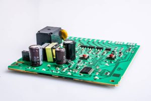
Suppose a panel contains three different PCB designs, but the order information does not specify that the PCB Panel contains three separate designs.
If the manufacturer’s engineering team does not identify the panelization intent correctly, production may be based on only one of the designs. The other two designs could be omitted completely, resulting in incorrect quantities and potentially delaying the production schedule.
How to Avoid the Problem
Always specify the exact number of different PCB designs contained in the panel.
For example, if one panel contains three PCB designs with different individual PCB data, the order information should clearly indicate:
Panelized PCB quantity: 3 designs
The important point is that the number of designs refers to the number of different PCB designs, not simply the number of boards physically arranged on the panel.
If the PCB designs are not completely identical, they should generally be treated as different designs, even when their overall dimensions are the same.
Small differences in:
- Hole locations
- Trace routing
- Pad positions
- Copper patterns
- Component placement
- Solder mask openings
can mean that the individual boards are different PCB designs.
For complex projects, professional PCB Design & Layout support can also help verify whether multiple boards have been correctly prepared for manufacturing.
2. Provide Complete Data for Reverse-Side Panelization
Reverse-side panelization, sometimes called an A-side/B-side or front-and-back panel arrangement, places different PCB designs on opposite sides of the same production panel.
Because this configuration involves different designs on the two sides, complete manufacturing data is especially important.
Common Reverse-Side Panelization Error
A common mistake is to provide only a panelization diagram showing which PCB is located on the front side and which PCB is located on the back side, without supplying the complete PCB design data.
A panel diagram can communicate the intended physical arrangement, but it does not contain all the manufacturing information required to fabricate the PCBs.
Without the complete PCB data, the manufacturer’s engineering team may not be able to accurately determine:
- Copper patterns
- Pad locations
- Drill holes
- Solder mask openings
- Silkscreen
- Board outlines
- Other critical manufacturing features
As a result, a panel intended to contain different designs on the two sides could potentially be interpreted as a conventional panel containing the same design.
How to Avoid the Problem
When submitting reverse-side panelization files, provide complete production data for every PCB included in the panel.
The manufacturing package should clearly define the required:
- Copper layers
- Pads
- Drill data
- Solder Mask Layer
- Silkscreen
- Board outlines
- Other required fabrication information
The panelization drawing should be used as supplementary information rather than as a replacement for the actual PCB manufacturing data.
A complete and clearly organized data package is particularly important when the project will proceed from prototype fabrication to PCB Assembly.
3. Keep PCB Panelization and Tooling Standards Consistent
The third critical consideration is the relationship between panelization and production tooling.
PCB panels may need to work with various tools and fixtures used during PCB assembly and testing, including:
- SMT stencils
- Test fixtures
- Assembly fixtures
- Post-SMT process fixtures
- Other production tooling
Therefore, the panel dimensions and tooling specifications must remain consistent throughout the manufacturing process.
Common Tooling Compatibility Error
A typical problem occurs when the customer prepares a panelized PCB and creates the required tooling before informing the manufacturer.
Different manufacturers may apply different manufacturing compensation factors or make adjustments to panel dimensions during production preparation.
If the final PCB panel dimensions differ from the dimensions used to manufacture the tooling, the previously manufactured stencil or fixture may no longer fit the PCB correctly.
This can result in:
- Tooling incompatibility
- Assembly delays
- Additional tooling costs
- Rework
- Production schedule disruptions
How to Avoid the Problem
If tooling has already been prepared, clearly inform the manufacturer when submitting the PCB order.
This information should be communicated before production begins so that the manufacturer’s engineering team can review the panel and tooling requirements together.
For new projects, it is generally safer to wait until the manufacturer has confirmed the final production data before manufacturing critical tooling.
This is especially important for SMT Tooling, where stencil dimensions and apertures need to correspond accurately to the final PCB panel and assembly requirements.
For high-volume production, consistent tooling and panel dimensions become even more important because a small dimensional mismatch can affect a large number of assembled boards.
Why PCB Panelization Matters in PCB Manufacturing
The purpose of panelization is not simply to place multiple boards onto a larger production panel.
Effective PCB Panelization is a process of accurately transferring design requirements into manufacturing information.
A successful panelization workflow should ensure that:
- The number of different PCB designs is clearly specified.
- Complete manufacturing data is provided for every PCB.
- Front-side and back-side designs are clearly identified when applicable.
- Panel dimensions are consistent with manufacturing requirements.
- Stencils and other tooling are based on the final approved production data.
- PCB fabrication and assembly requirements remain synchronized.
When these details are handled correctly, manufacturers can process the order with fewer uncertainties and reduce the risk of production errors.
Verify Panelization Before Mass Production
Before moving a project into production, engineers should perform a final review of the panelized manufacturing package.
The review should confirm that the Gerber files, drill files, panel drawing, board quantity, PCB designs, and tooling requirements are consistent.
For projects requiring both fabrication and assembly, the panel should also be reviewed against the assembly process to ensure that the selected panel configuration supports efficient production.
A properly prepared panel can improve manufacturing efficiency, while an incorrectly defined panel can create problems that propagate into fabrication, assembly, inspection, and delivery.
Conclusion
The key to successful PCB panelization is accurate communication between design requirements and manufacturing data.
The three most important points are simple:
- Specify the exact number of different PCB designs in the panel.
- Provide complete manufacturing data for reverse-side panelization.
- Ensure that panel dimensions and tooling standards remain consistent.
PCB production depends on precise and consistent information. Even a small discrepancy in panelization data can lead to missing designs, incorrect production, or tooling incompatibility.
By verifying these three details before production, engineers can significantly reduce panelization risks and create a more reliable path from PCB design to assembly and mass production.
In short, successful PCB Manufacturing is not only about producing the board itself. It also depends on ensuring that every piece of production information—from panelization to tooling—is accurate, complete, and consistent.