4-Layer PCB Stackup: PCB Design, PCB Manufacturing & Design Guide
As modern electronic products become smaller, faster, and more functionally integrated, printed circuit boards (PCBs) must accommodate higher component density, faster signal speeds, improved power distribution, and stronger electromagnetic compatibility (EMC) performance.
A 4-Layer PCB provides a practical solution between a conventional two-layer board and a more complex multilayer PCB. By adding dedicated internal layers for power, ground, or signal routing, a four-layer board can provide more routing resources and better reference-plane management than a two-layer PCB.
A well-designed 4-layer stackup can also improve signal integrity, reduce unwanted electromagnetic radiation, simplify power distribution, and provide a more controlled environment for high-speed interfaces.
This guide explains the 4-Layer PCB Stackup, layer configuration, PCB Design considerations, manufacturing process, applications, advantages, cost factors, and key differences between 2-layer and 4-layer PCBs.
What Is a 4-Layer PCB?
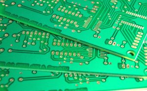
A 4-Layer PCB is a multilayer printed circuit board containing four copper layers separated by dielectric materials.
A common four-layer configuration is:
- Top Layer – Signal
- Inner Layer 1 – Ground
- Inner Layer 2 – Power or Signal
- Bottom Layer – Signal
Another common configuration uses the two internal layers primarily for ground and power distribution.
Unlike a two-layer PCB, a four-layer PCB can dedicate one or more internal layers to relatively continuous reference planes. This makes it easier to provide controlled return paths and power distribution while keeping signal routing on the outer layers.
Compared with a six-layer PCB, a four-layer PCB generally has fewer routing resources and fewer options for separating multiple signal and power domains, but it can offer a simpler and potentially lower-cost construction when four layers are sufficient for the design.
The actual electrical performance depends heavily on the stackup geometry, dielectric material, trace dimensions, routing strategy, component placement, and operating frequency.
4-Layer PCB Stackup Explained
The stackup is one of the most important aspects of PCB Design.
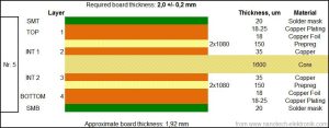
A typical 4-layer PCB contains:
- Top copper foil
- Prepreg dielectric
- Inner copper layer
- Core dielectric
- Inner copper layer
- Prepreg dielectric
- Bottom copper foil
A representative structure can be arranged as follows:
| Layer | Typical Function | Typical Material |
|---|---|---|
| Layer 1 | Signal / component layer | Copper |
| Dielectric | Insulation | FR-4 prepreg |
| Layer 2 | Ground plane | Copper |
| Core | Insulation | FR-4 core |
| Layer 3 | Power / signal plane | Copper |
| Dielectric | Insulation | FR-4 prepreg |
| Layer 4 | Signal / component layer | Copper |
This is only one possible configuration. The correct stackup depends on signal-speed requirements, impedance targets, copper thickness, dielectric thickness, thermal requirements, manufacturability, and cost.
Why Is the Stackup Important?
The distance between a signal trace and its reference plane directly affects its characteristic impedance.
A carefully engineered stackup can therefore help control:
- Trace impedance
- Return-current paths
- Crosstalk
- Electromagnetic radiation
- Power distribution
- Signal propagation
- Thermal performance
For high-speed designs, stackup planning should be completed before detailed routing begins.
Common 4-Layer PCB Stackup Configurations
There are several practical ways to configure a four-layer PCB.
Configuration 1: Signal – Ground – Power – Signal
This is a common arrangement for mixed-signal and digital designs.
The two outer layers provide convenient component placement and signal routing, while the internal layers provide relatively continuous ground and power distribution.
Advantages include:
- Short signal return paths
- Improved power distribution
- Better EMI control
- Convenient external-layer routing
Configuration 2: Signal – Ground – Ground – Signal
This configuration provides two internal reference planes, although one or both may be partitioned or assigned according to the application.
It can be useful when signal integrity and return-path control are major priorities.
Configuration 3: Signal – Signal – Ground – Signal
Some four-layer designs allocate three layers primarily for signals and one layer for ground.
Although this provides additional routing resources, it requires careful return-path management because not every signal layer is immediately adjacent to a solid reference plane.
The best configuration depends on the electrical requirements rather than simply the number of layers.
4-Layer PCB Manufacturing Process
A standard four-layer PCB can generally be manufactured using a conventional multilayer PCB fabrication process without requiring sequential lamination.
The basic PCB Manufacturing workflow includes the following steps.
Step 1 – Inner-Layer Imaging
The copper on the inner core is cleaned and coated with photoresist.
The circuit pattern is transferred onto the copper using imaging equipment.
Step 2 – Inner-Layer Etching
Unwanted copper is removed through an etching process.
The remaining copper forms the inner signal, ground, or power structures.
Step 3 – Inner-Layer Inspection
The fabricated inner layers are inspected using processes such as Automated Optical Inspection (AOI).
The inspection verifies:
- Trace width
- Trace spacing
- Open circuits
- Shorts
- Copper defects
- Pattern accuracy
Step 4 – Layup and Lamination
The inner core, prepreg, and outer copper foils are carefully aligned.
The complete stackup is then laminated under controlled temperature and pressure.
During lamination, the prepreg softens and flows, bonding the layers into a single multilayer PCB structure.
Step 5 – Drilling
After lamination, holes are drilled through the PCB.
For a conventional four-layer PCB, these commonly include:
- Plated through-holes
- Component holes
- Mounting holes
- Other mechanical holes
Blind or buried vias can also be used, but they add manufacturing complexity and are not required for most standard four-layer designs.
Step 6 – Hole Metallization
The drilled holes are cleaned and prepared for copper deposition.
Electroless copper is deposited onto the hole walls, followed by electrolytic copper plating.
This creates conductive paths connecting the required PCB layers.
Step 7 – Outer-Layer Imaging and Etching
The outer copper layers are patterned to create:
- Signal traces
- Pads
- Ground areas
- Power connections
Step 8 – Solder Mask and Surface Finish
Solder mask is applied to protect exposed copper and reduce the risk of solder bridges.
Common surface finishes include:
- ENIG
- HASL
- OSP
- Immersion tin
- Immersion silver
The appropriate finish depends on the assembly process, component requirements, reliability requirements, and cost targets.
Step 9 – Electrical Testing and Inspection
Final inspection may include:
- AOI
- Electrical continuity testing
- Isolation testing
- Flying-probe testing
- Fixture-based testing
- Dimensional inspection
- Impedance testing where required
For high-speed designs, impedance coupons can be fabricated and tested to verify that the manufacturing process achieves the specified impedance targets.
4-Layer PCB Design Considerations
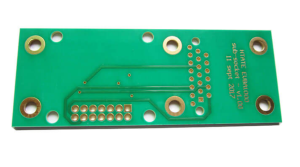
A successful 4-Layer PCB Design must consider electrical, mechanical, thermal, and manufacturing requirements simultaneously.
1. Return Paths and Current Loops
High-speed signals require well-controlled return-current paths.
Whenever possible, high-speed traces should be routed adjacent to a continuous reference plane.
Designers should avoid unnecessary plane splits underneath high-speed signal traces because they can force return currents to take longer paths.
This can increase loop area and contribute to:
- EMI
- Crosstalk
- Ground noise
- Signal integrity problems
2. Component Placement and Decoupling
Decoupling capacitors should be placed close to the relevant IC power pins.
The connection between the capacitor, power pin, and ground should be as short and low-inductance as practical.
Good placement reduces the parasitic inductance of the power-delivery path and improves high-frequency power integrity.
Sensitive analog circuitry should also be separated appropriately from noisy digital or switching circuits.
However, this does not necessarily mean physically splitting the ground plane. In many designs, maintaining a continuous reference plane and controlling current return paths is preferable to creating unnecessary plane gaps.
3. Controlled Impedance
Controlled impedance is important for many high-speed interfaces.
The impedance depends on factors such as:
- Trace width
- Trace thickness
- Dielectric thickness
- Dielectric constant
- Reference-plane geometry
- Copper roughness
- Manufacturing tolerances
Therefore, impedance should be calculated from the actual proposed stackup rather than using a generic trace-width rule.
Common interfaces that may require impedance control include:
- USB
- Ethernet
- HDMI
- PCI Express
- MIPI
- RF interfaces
- High-speed memory interfaces
4. Via Strategy
Vias provide electrical connections between PCB layers, but every via introduces parasitic capacitance and inductance.
For high-speed routing:
- Minimize unnecessary layer transitions.
- Avoid long via stubs.
- Keep return paths continuous.
- Use ground stitching vias where appropriate.
- Consider via-in-pad or backdrilling only when justified by the electrical requirements and manufacturing capability.
Backdrilling can reduce the unused via barrel below the active signal layers, but it is generally more relevant to higher-speed multilayer designs where via stubs materially affect signal integrity.
5. Differential Pair Routing
Differential signals should be routed with consistent geometry.
Important considerations include:
- Controlled differential impedance
- Trace width
- Differential spacing
- Length matching where required
- Reference-plane continuity
- Avoidance of unnecessary vias
- Consistent routing environment
Length matching should be based on the interface timing requirements rather than applied indiscriminately to every differential pair.
6. Thermal Management
Although four-layer PCBs provide fewer thermal options than some higher-layer boards, they can still provide effective thermal management.
Copper planes can distribute heat across the board, while thermal vias can transfer heat from component pads into internal copper areas.
Thermal design should consider:
- Component power dissipation
- Copper area
- Via density
- PCB thickness
- Airflow
- Enclosure conditions
- Ambient temperature
High-power components may require additional thermal solutions beyond the PCB itself.
Glass-Weave Effects in 4-Layer PCB Design
High-speed PCB designers should also consider dielectric anisotropy caused by the fiberglass weave in laminate materials.
The resin-rich and glass-rich regions can have different effective dielectric properties. When a high-speed trace runs in an unfavorable relationship to the glass weave, propagation delay and impedance can vary across the trace.
This effect can become relevant in high-speed differential designs.
Potential mitigation techniques include:
- Trace routing relative to the glass weave
- Using spread-weave or low-Dk fabric constructions
- Adjusting trace geometry
- Increasing dielectric uniformity
- Working with the laminate supplier on material selection
The commonly used 2116 and 7628 glass styles have different construction characteristics, but simply specifying one glass style does not automatically eliminate glass-weave effects.
Applications of 4-Layer PCBs
Four-layer PCBs are widely used in applications requiring more routing density and better power and signal management than a basic two-layer board.
Consumer Electronics and Communications
Typical applications include:
- Routers
- Wireless modules
- Wearable electronics
- Smart-home devices
- Consumer controllers
- Communication equipment
A four-layer structure provides additional routing resources while remaining relatively compact.
Automotive and Industrial Electronics
Four-layer PCBs can be found in:
- Sensors
- Electronic control modules
- Power-control circuits
- Instrumentation
- Industrial controllers
- Motor-control electronics
The actual layer count depends on the circuit complexity, power level, signal-speed requirements, and environmental requirements.
IoT Devices
IoT products often need to combine:
- Microcontrollers
- Wireless communication
- Sensors
- Power-management circuits
- Memory
- User interfaces
A four-layer PCB can provide enough routing and grounding resources for many such compact systems.
Medical Electronics
Four-layer PCBs can be used in various medical and healthcare products, including:
- Portable monitors
- Blood-pressure monitors
- Glucose meters
- Pulse oximeters
- Diagnostic equipment
- Portable sensing devices
Medical PCB requirements depend heavily on the device type, risk classification, applicable regulations, and electrical safety requirements.
4-Layer PCB vs. 2-Layer PCB
The main differences between two-layer and four-layer PCBs are related to routing capacity, reference-plane availability, electrical performance, manufacturing complexity, and cost.
| Feature | 2-Layer PCB | 4-Layer PCB |
|---|---|---|
| Copper layers | 2 | 4 |
| Routing resources | More limited | Higher |
| Dedicated reference plane | More difficult | Easier to implement |
| Power distribution | More constrained | More flexible |
| Return-path control | More challenging | Generally easier |
| EMI management | Design-dependent | More opportunities for controlled return paths |
| High-speed design | Possible with careful design | Often easier to implement |
| Manufacturing cost | Generally lower | Generally higher |
| Design complexity | Lower | Moderate |
| Typical applications | Simple to moderately complex circuits | More dense and electrically demanding designs |
A four-layer PCB is not automatically better for every application. If a circuit is electrically simple and does not require additional routing or reference-plane control, a two-layer PCB may be sufficient.
Advantages of 4-Layer PCBs
Increased Routing Capacity
Four copper layers provide substantially more routing resources than a two-layer board.
Designers can use the external layers for components and signal routing while allocating internal layers to ground, power, or additional signal routing.
This can make dense component escape routing easier.
Better Signal Integrity
A continuous reference plane can provide a shorter and more predictable return path for high-speed signals.
This can help reduce:
- Loop area
- Crosstalk
- Uncontrolled radiation
- Ground noise
- Signal discontinuities
The improvement depends on the actual stackup and layout quality.
Better Power Distribution
An internal power plane or dedicated copper region can distribute power more efficiently than long power traces.
Combining power distribution with closely placed ground planes can also reduce power-distribution impedance.
More Compact Layout
Additional copper layers allow designers to route more signals without making the board excessively large.
This is particularly useful for:
- High-pin-count ICs
- Fine-pitch packages
- Compact consumer products
- Embedded controllers
- Wireless modules
Improved EMI/EMC Design Flexibility
A continuous ground plane can help control current return paths and reduce unnecessary loop areas.
This gives four-layer designs more flexibility for electromagnetic compatibility than many simple two-layer layouts.
4-Layer PCB Cost Factors
The cost of a four-layer PCB depends on both the board specification and the manufacturing process.
Board Size
Larger PCBs consume more laminate and copper and may reduce panel utilization.
Material Selection
Standard FR-4 is often used for general-purpose four-layer boards.
High-Tg, low-loss, halogen-free, or specialty laminates can increase material costs but may be necessary for specific electrical, thermal, or environmental requirements.
Copper Thickness
Higher copper weights increase material usage and may require additional plating and etching considerations.
Surface Finish
ENIG, OSP, HASL, immersion silver, and immersion tin have different processing requirements and costs.
Via Technology
Standard through-hole vias are generally simpler to manufacture.
Blind vias, buried vias, via-in-pad structures, and other advanced via technologies can increase fabrication complexity.
Board Quantity
Prototype and low-volume production generally have higher unit costs because setup and engineering expenses are distributed across fewer boards.
Larger production quantities can reduce unit cost when the design and manufacturing process are stable.
Panel Utilization
Panelization efficiency can have a significant influence on unit cost.
Factors include:
- PCB dimensions
- Array configuration
- Routing clearance
- Tooling
- Breakaway method
- Manufacturing yield
How to Optimize a 4-Layer PCB for Manufacturing
A successful four-layer board requires cooperation between the designer and PCB manufacturer.
Before releasing the design for production, engineers should verify:
- Final layer stackup
- Copper thickness
- Dielectric thickness
- Controlled impedance requirements
- Minimum trace width
- Minimum spacing
- Hole diameter
- Annular ring
- Solder-mask clearance
- Surface finish
- PCB thickness
- Panelization
- Manufacturing tolerances
A professional DFM review can identify potential fabrication problems before production begins.
For high-speed designs, the manufacturer should also confirm whether the selected stackup and materials can achieve the specified single-ended and differential impedance targets.
Conclusion
A 4-Layer PCB provides a practical balance between routing density, electrical performance, manufacturing complexity, and cost.
By incorporating two additional copper layers, designers can allocate internal layers for ground, power, or signal routing and create better-controlled electrical environments than many conventional two-layer designs.
The most important benefits include increased routing capacity, improved return-path management, better power distribution, enhanced signal integrity, and greater flexibility for EMI/EMC control.
However, simply increasing the number of PCB layers does not automatically guarantee better performance. The actual result depends on the 4-Layer PCB Stackup, dielectric thickness, trace geometry, reference-plane continuity, component placement, via strategy, thermal design, and manufacturing tolerances.
For modern consumer electronics, IoT products, automotive electronics, industrial controllers, communication equipment, and many medical devices, a properly engineered four-layer board can provide an effective foundation for reliable and manufacturable electronic products.
Article Summary
A 4-layer PCB contains four copper layers separated by dielectric materials and provides more routing resources and reference-plane options than a two-layer PCB. A well-designed 4-Layer PCB Stackup can improve power distribution, signal integrity, return-path control, and EMI/EMC performance. Successful PCB Design requires careful attention to stackup, impedance, differential pairs, vias, component placement, thermal management, and glass-weave effects. During PCB Manufacturing, accurate lamination, drilling, plating, imaging, solder-mask application, surface finishing, AOI, and electrical testing are essential to achieving consistent production quality.