6-Layer PCB: PCB Design, PCB Manufacturing, Stackup, Benefits & Applications
A 6-Layer PCB is a multilayer printed circuit board containing six conductive copper layers separated by dielectric materials and bonded together through a controlled lamination process. Compared with two-layer and four-layer boards, a six-layer configuration provides more routing resources, additional reference planes, improved power distribution, and greater flexibility for managing signal integrity and electromagnetic compatibility.
Six-layer boards are widely used in telecommunications, automotive electronics, industrial equipment, computing systems, networking devices, and other applications where routing density and electrical performance must be balanced with board size and manufacturing cost.
For high-speed designs, the stackup is particularly important. Signal layers must have appropriate reference planes and dielectric spacing to control impedance and provide predictable return-current paths. An impedance discontinuity can cause reflections, additional insertion loss, crosstalk, and signal-integrity problems, especially in multi-gigabit systems.
This article explains what a 6-Layer PCB is, how a six-layer stackup works, its advantages, material and thickness options, manufacturing process, design guidelines, cost factors, and how to select a reliable 6-Layer PCB Manufacturing partner.
What Is a 6-Layer PCB?
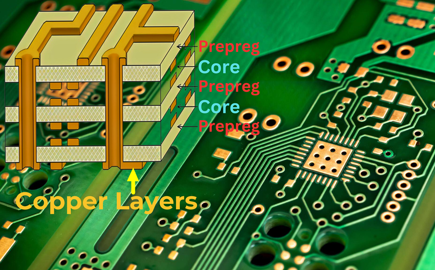
A six-layer printed circuit board contains six copper layers separated by dielectric materials such as core and prepreg. The copper layers may function as signal layers, power planes, or ground planes depending on the application.
A typical six-layer structure may provide four signal layers and two reference or power-related layers, although many other configurations are possible.
The primary benefit is not simply the number of copper layers. A well-engineered 6-Layer PCB Design uses the additional layers strategically to:
- Increase routing capacity
- Provide continuous reference planes
- Improve signal-return paths
- Support controlled-impedance routing
- Reduce crosstalk
- Improve power integrity
- Reduce EMI
- Simplify high-density component routing
- Separate sensitive analog, digital, and power circuits where appropriate
For high-speed applications, the relationship between signal traces and their reference planes is especially important. A signal layer placed close to a continuous ground plane can provide a more predictable return path and help reduce electromagnetic radiation.
However, simply adding a ground or power layer does not automatically guarantee better performance. The complete stackup, dielectric thickness, copper geometry, component placement, via structures, and routing strategy must be considered together.
Typical 6-Layer PCB Stackup
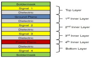
The PCB stackup directly affects impedance, signal integrity, EMI/EMC behavior, thermal characteristics, and manufacturability.
There is no single stackup that is ideal for every six-layer board. The correct configuration depends on the signal-speed requirements, layer utilization, impedance targets, component density, power distribution, material selection, and fabrication capabilities.
Standard 6-Layer Stackup Example
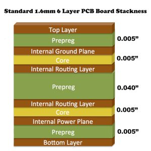
One commonly used six-layer arrangement is:
Signal – Ground – Signal – Power/Ground – Ground – Signal
Another possible configuration is:
Signal – Ground – Signal – Signal – Power – Signal
The appropriate structure depends on the design requirements.
For high-speed systems, the key consideration is to ensure that important signal layers have nearby, continuous reference planes. If a high-speed trace changes reference planes or crosses a split plane, its return current may be forced to take a longer path, increasing loop inductance and potentially causing EMI and signal-integrity problems.
Example Engineering Stackup
| Layer | Type | Primary Function | Design Considerations |
|---|---|---|---|
| L1 | Signal | Component-side routing | High-speed and critical signals |
| L2 | Ground | Reference plane | Return-current path and EMI control |
| L3 | Signal | Internal routing | Controlled-impedance signals |
| L4 | Signal / Power | Internal routing or power distribution | Depends on system architecture |
| L5 | Ground / Power | Reference or power plane | Power integrity and return path |
| L6 | Signal | Bottom-side routing | Component and low-/medium-speed connections |
This is only an example. A 6-Layer PCB Stackup should be developed around the actual electrical and mechanical requirements rather than copied as a universal template.
Why Stackup Symmetry Matters
A reasonably balanced and mechanically symmetrical stackup can help reduce warpage and mechanical stress during lamination and subsequent thermal processing.
However, stackup symmetry does not mean every six-layer board must use perfectly identical dielectric thicknesses or copper weights. Electrical requirements sometimes require an intentionally asymmetric structure.
The important principle is to balance mechanical reliability with signal-integrity and manufacturing requirements.
Controlled Impedance in 6-Layer PCB Design
Controlled impedance is one of the most important considerations in high-speed PCB Design.
Common target values include 50 Ω for many single-ended RF and high-speed interfaces and 90 Ω or 100 Ω for various differential interfaces. The exact target depends on the interface specification and system architecture.
Impedance is influenced by:
- Trace width
- Trace thickness
- Copper roughness
- Dielectric thickness
- Dielectric constant
- Trace geometry
- Reference-plane configuration
- Solder mask
- Operating frequency
Therefore, changing the dielectric thickness or copper thickness can change the impedance even when the PCB layout itself remains unchanged.
Advanced PCB engineering workflows use 2D field solvers or stackup calculators to estimate impedance before fabrication. For critical designs, the manufacturer can then verify the stackup and provide impedance-control coupons for production validation.
Benefits of Using a 6-Layer PCB
A well-designed six-layer board provides several technical advantages over lower-layer-count PCBs.
1. Higher Routing Density
Six copper layers provide substantially more routing resources than two- or four-layer boards.
This is particularly useful for products containing high-pin-count processors, memory devices, FPGAs, connectors, communication interfaces, and other dense components.
Additional routing layers can reduce congestion without requiring a significant increase in board dimensions.
2. Improved Signal Integrity
A carefully designed six-layer stackup can place critical signal layers close to continuous reference planes.
This helps reduce return-path discontinuities and can improve control over impedance and electromagnetic coupling.
For high-speed interfaces, maintaining a predictable signal-return path is often more important than simply increasing the number of routing layers.
3. Better EMI and Crosstalk Control
Ground planes can provide effective reference structures around signal layers and reduce unwanted coupling between traces.
However, a ground plane should not be considered a universal EMI shield by itself. Proper component placement, return-path design, trace spacing, via stitching, power distribution, and enclosure-level EMC design are also important.
4. Greater Design Flexibility
Six layers allow engineers to allocate routing resources more effectively.
For example, one or more layers can be dedicated primarily to high-speed signals while other layers accommodate power distribution, lower-speed signals, or sensitive analog circuits.
This flexibility can make complex board layouts easier to manage.
5. Improved Power Integrity
Dedicated power and ground structures can help reduce distribution impedance and improve power-delivery performance.
A tightly coupled power-ground structure can also contribute to lower AC impedance over relevant frequency ranges.
Nevertheless, decoupling capacitors, plane geometry, current paths, and regulator placement remain critical to power integrity.
6. Better Thermal Management
Copper planes can spread heat away from components and distribute thermal energy across a larger area.
Six-layer boards provide more copper area than simpler boards, although actual thermal performance depends on copper thickness, copper area, vias, component power dissipation, airflow, and enclosure design.
For high-power applications, thermal vias and dedicated heat-spreading structures may be required.
7. Support for Complex High-Speed Systems
With suitable stackup design and manufacturing controls, six-layer boards can support demanding digital, RF, networking, automotive, and industrial applications.
The board’s actual speed capability depends on the complete design rather than layer count alone.
6-Layer PCB Thickness and Material Options
The thickness and material selection of a 6-Layer PCB affect mechanical strength, electrical performance, thermal behavior, manufacturability, and cost.
PCB Thickness
A 1.6 mm finished thickness is common for many standard multilayer PCBs, but six-layer boards can be manufactured in thinner or thicker constructions depending on the application and manufacturing capabilities.
For example:
- Approximately 0.8–1.0 mm: compact and lightweight applications
- Approximately 1.2 mm: space-constrained electronics
- Approximately 1.6 mm: common general-purpose construction
- Approximately 2.0 mm or more: applications requiring additional mechanical rigidity
The actual finished thickness depends on copper weights, core thicknesses, prepreg selection, and the manufacturer’s lamination process.
FR-4 and High-Tg Materials
FR-4 is widely used for six-layer boards because it provides a good balance between electrical performance, mechanical properties, manufacturability, and cost.
Standard FR-4 materials may have Tg values around 130°C or higher depending on the material system. High-Tg laminates are also available for applications requiring improved thermal reliability.
It is important to remember that Tg is not the maximum continuous operating temperature of the PCB. Thermal reliability depends on the complete laminate system, processing conditions, copper construction, component temperatures, and application environment.
High-Frequency Laminates
When a six-layer PCB contains RF or microwave circuits, specialized low-loss laminates may be considered.
Materials from suppliers such as Rogers, Panasonic, Isola, and Taconic can be selected when their electrical properties meet the application’s frequency, loss, impedance, and environmental requirements.
A hybrid stackup may also be used, combining conventional FR-4-family materials with specialized RF laminates where appropriate.
Copper Weight
Common copper weights include 1 oz and 2 oz, corresponding approximately to 35 µm and 70 µm of copper before processing.
Higher copper weights can support greater current capacity and heat spreading, but thicker copper also affects etching, minimum trace width, via design, impedance, and manufacturing cost.
Therefore, copper thickness should be selected according to both electrical requirements and fabrication capability.
6-Layer PCB Manufacturing Process
The 6-Layer PCB Manufacturing process involves multiple controlled stages. Layer registration, lamination quality, drilling accuracy, copper plating, surface finish, and electrical testing all contribute to the final product.
1. Inner-Layer Fabrication
The inner copper layers are cleaned and coated with photoresist.
The required circuit patterns are transferred using imaging technology, followed by development and etching.
After etching, the inner layers are inspected to verify trace width, spacing, defects, and pattern accuracy.
2. Inner-Layer Inspection
Automated optical inspection (AOI) can be used to identify potential defects such as:
- Open circuits
- Shorts
- Missing copper
- Excess copper
- Pattern deviations
- Foreign material
The inner layers must meet the required specifications before lamination.
3. Lamination
The inner cores, prepreg sheets, and copper foils are stacked according to the specified stackup.
Heat and pressure are applied according to the laminate manufacturer’s process window so that the resin flows and bonds the layers together.
The exact lamination temperature and pressure depend on the selected material system and resin characteristics. Therefore, a universal temperature such as 170–190°C should not be treated as a requirement for every six-layer PCB.
Controlled lamination is essential for:
- Layer bonding
- Dimensional stability
- Registration
- Void reduction
- Delamination resistance
- Long-term reliability
4. Drilling and Via Formation
After lamination, holes are drilled to create electrical connections between the required layers.
Depending on the construction, the board may use:
- Through vias
- Blind vias
- Buried vias
- Microvias
Mechanical drilling is widely used for conventional through-holes, while laser drilling may be used for microvias and certain HDI structures.
Laser drilling is not inherently better than mechanical drilling. The appropriate process depends on via dimensions, stackup architecture, aspect ratio, production volume, and cost requirements.
5. Desmear and Copper Plating
After drilling, the hole walls are prepared and treated to ensure reliable copper adhesion.
Electroless copper deposition creates a conductive layer on the hole walls, followed by electrolytic copper plating to achieve the required copper thickness.
6. Outer-Layer Imaging and Etching
The external circuit patterns are transferred onto the outer copper layers.
The unwanted copper is then removed through controlled etching, leaving the final traces, pads, and other conductive features.
7. Solder Mask and Silkscreen
A solder mask is applied to protect exposed copper and reduce the risk of solder bridging.
Silkscreen markings can then be added to identify component references, polarity, connectors, and other assembly information.
8. Surface Finish
The exposed copper pads receive a suitable surface finish.
Common options include:
- ENIG
- HASL
- Lead-free HASL
- OSP
- Immersion tin
- Immersion silver
The best finish depends on solderability, shelf life, contact requirements, cost, flatness, and environmental conditions.
9. Electrical Testing and Inspection
Finished six-layer boards can undergo several inspection and testing processes, including:
- AOI
- Electrical continuity and isolation testing
- Flying-probe testing
- Dimensional inspection
- Solder-mask inspection
- Surface-finish inspection
- Impedance testing
- Microsection analysis
- X-ray inspection where appropriate
For controlled-impedance products, test coupons can be incorporated into the production panel to verify that impedance remains within the specified tolerance.
6-Layer PCB Manufacturing Tolerances
Manufacturing tolerances must be defined according to the manufacturer’s capabilities and the PCB design requirements.
It is not appropriate to assign one universal drill tolerance, layer-registration tolerance, or minimum trace/space value to every six-layer board.
For example, conventional six-layer PCBs may support larger design rules than advanced HDI constructions, while high-density products may require much tighter geometries.
Typical project specifications may include:
| Parameter | Example Range / Target |
|---|---|
| Finished board thickness | Application-dependent |
| Copper weight | 1–2 oz commonly used |
| Controlled impedance | Commonly 50 Ω, 90 Ω, or 100 Ω depending on interface |
| Minimum trace/space | Application and manufacturing capability dependent |
| Drill tolerance | Manufacturer and hole-size dependent |
| Layer registration | Stackup and fabrication capability dependent |
| Impedance tolerance | Often specified by customer requirement |
The manufacturer should confirm the achievable tolerances during DFM review rather than relying on generic numbers.
6-Layer PCB Design Guidelines
A successful 6-Layer PCB Design requires electrical, mechanical, and manufacturing considerations to be addressed simultaneously.
1. Define the Stackup Early
The stackup should be established before final routing begins.
Engineers should define:
- Number of signal layers
- Ground-plane locations
- Power-plane locations
- Dielectric thickness
- Copper thickness
- Target impedance
- Material selection
Changing the stackup late in the design can require significant routing changes.
2. Maintain Continuous Reference Planes
High-speed traces should have a continuous reference plane wherever practical.
Avoid routing critical signals across plane splits or areas where the reference structure changes unexpectedly.
3. Optimize Return Paths
The return current of a high-frequency signal tends to follow a path associated with the electromagnetic field and reference structure.
Therefore, a short, continuous return path is essential for signal integrity and EMI control.
4. Control Differential Pairs
Differential pairs should be routed according to the requirements of the relevant interface.
Maintain appropriate:
- Trace width
- Pair spacing
- Length matching
- Reference-plane relationship
- Via transitions
Do not assume that every differential interface requires exactly 100 Ω; the target depends on the interface specification.
5. Minimize Unnecessary Via Transitions
Every via can introduce parasitic capacitance, inductance, and impedance discontinuity.
However, vias should not be eliminated at the expense of poor routing or poor reference-plane continuity. The objective is to use an appropriate via strategy.
6. Separate Noisy and Sensitive Circuits
Power switching circuits, high-current paths, analog circuits, clocks, and high-speed digital interfaces can create different types of electromagnetic interference.
Thoughtful placement and routing can reduce unwanted coupling.
7. Use DFM and DRC Early
Design Rule Check (DRC) and Design for Manufacturing (DFM) analysis should be performed before the design is released for production.
Early review can identify:
- Insufficient copper spacing
- Difficult drill structures
- Acid traps
- Unmanufacturable features
- Impedance problems
- Insufficient solder-mask clearance
- Poor annular rings
- Stackup-related issues
8. Perform Signal-Integrity Simulation
For high-speed six-layer designs, simulation tools can help evaluate:
- Impedance
- Reflection
- Crosstalk
- Insertion loss
- Return loss
- Timing
- Eye diagrams
- Power integrity
SPICE is useful for circuit-level analysis, while electromagnetic field solvers and dedicated SI/PI tools are more appropriate for transmission-line and interconnect analysis.
6-Layer PCB Technical Specifications
The technical specifications of a six-layer PCB should be defined according to the project rather than relying on a universal specification.
A typical specification sheet may include:
| Specification | Typical Consideration |
|---|---|
| Layer count | 6 conductive layers |
| Board thickness | Approximately 0.8–2.0 mm or project-specific |
| Material | FR-4, high-Tg FR-4, low-loss laminate, etc. |
| Copper thickness | Commonly 1–2 oz, application dependent |
| Surface finish | ENIG, HASL, OSP, immersion tin, etc. |
| Controlled impedance | 50 Ω / 90 Ω / 100 Ω as required |
| Minimum trace/space | Based on design and fabrication capability |
| Via structure | Through, blind, buried, or microvia as required |
| Testing | AOI, electrical test, impedance test, X-ray where appropriate |
6-Layer PCB vs 4-Layer PCB
The decision between four and six layers depends on routing density, signal-integrity requirements, power distribution, board dimensions, and cost.
| Feature | 6-Layer PCB | 4-Layer PCB |
|---|---|---|
| Routing capacity | Higher | Lower |
| Layer allocation flexibility | Higher | Moderate |
| High-speed routing | More flexible | More constrained |
| Reference-plane options | More | Fewer |
| EMI/return-path management | More flexible | More constrained |
| Power distribution | More options | More limited |
| Manufacturing cost | Generally higher | Generally lower |
| Design complexity | Higher | Lower |
| Typical applications | Networking, industrial, automotive, computing | Consumer, control, embedded systems |
A six-layer board is not automatically superior to a four-layer board. If a four-layer design can meet the electrical, mechanical, thermal, and manufacturing requirements, additional layers may not provide sufficient value to justify the added cost.
6-Layer PCB Cost Factors
The cost of a six-layer board is influenced by more than the number of copper layers.
Material Cost
Standard FR-4 is generally more economical than specialized low-loss or high-temperature laminate systems.
Material cost also depends on:
- Board thickness
- Copper weight
- Laminate grade
- Panel utilization
- Surface finish
- Special materials
- HDI structures
Manufacturing Complexity
Six-layer boards require additional processing compared with simpler PCBs.
Cost can increase when the design requires:
- Fine lines and spaces
- High layer-registration accuracy
- Blind or buried vias
- Microvias
- Heavy copper
- Controlled impedance
- Special surface finishes
- Advanced inspection
- Tight dimensional tolerances
Panelization and Material Utilization
Efficient panelization can reduce material waste and lower the cost per board.
During DFM review, manufacturers can evaluate board orientation, spacing, tooling requirements, and panel utilization to improve manufacturing efficiency.
Design Optimization
Good PCB Design can directly influence manufacturing cost.
Reducing unnecessary complexity, avoiding unnecessarily tight tolerances, optimizing via structures, and selecting materials according to actual requirements can help achieve a better balance between performance and cost.
How to Choose a 6-Layer PCB Manufacturer
Selecting a reliable 6-Layer PCB Manufacturer requires evaluating both technical capability and production quality.
Consider the following factors:
Manufacturing Capability
Confirm whether the manufacturer can support:
- Six-layer multilayer fabrication
- Controlled impedance
- Fine-line routing
- High-Tg materials
- Low-loss RF materials where required
- Blind and buried vias
- Microvias when necessary
- Different copper weights
- Multiple surface finishes
Engineering Support
A strong engineering process should include DFM review, stackup analysis, impedance calculation, and manufacturability feedback.
This is especially important for high-speed six-layer boards because a small change in dielectric thickness or trace geometry can affect impedance.
Inspection and Testing
Evaluate the manufacturer’s capabilities for:
- AOI
- Electrical testing
- X-ray inspection
- Microsection analysis
- Impedance testing
- Dimensional inspection
- Material traceability
The appropriate inspection plan should be determined by the product’s reliability requirements.
Quality Management
For demanding applications, manufacturers should have documented process controls and quality systems appropriate to the customer’s industry and product requirements.
Relevant IPC standards and customer-specific specifications should be identified during project kickoff.
Kingda 6-Layer PCB Manufacturing Support
Kingda can support custom six-layer PCB projects from engineering review through PCB Manufacturing.
For a six-layer design, important project information includes the required layer stackup, finished thickness, copper weight, material type, impedance targets, minimum trace/space, via structure, surface finish, and testing requirements.
For high-speed, automotive, industrial, telecommunications, and other demanding applications, the PCB structure should be optimized around the actual electrical and mechanical requirements rather than using a generic six-layer stackup.
Kingda can work with customers to evaluate manufacturability, material selection, stackup configuration, impedance requirements, and production considerations for custom multilayer PCB projects.
Conclusion
A 6-Layer PCB provides a useful balance between routing density, signal integrity, power distribution, EMI control, mechanical requirements, and manufacturing cost.
Its six copper layers provide substantially more design flexibility than lower-layer-count boards, making six-layer configurations suitable for complex electronic systems.
However, simply adding two additional copper layers does not automatically improve PCB performance. The actual results depend on the stackup architecture, reference-plane continuity, dielectric thickness, material properties, copper geometry, via structures, component placement, and manufacturing quality.
For demanding applications, successful PCB Design and PCB Manufacturing should therefore be treated as a combined engineering process. A properly optimized six-layer board can provide reliable electrical performance while maintaining a practical balance between complexity, manufacturability, and cost.