GPS Module PCB Design Guide: Antenna Layout, RF Routing, Power, Grounding, and EMI Control
Designing a reliable GPS Module PCB requires much more than connecting a GPS receiver to a microcontroller. The RF section, antenna, power supply, grounding strategy, PCB stack-up, signal routing, thermal management, and manufacturing process all influence positioning accuracy and receiver sensitivity.
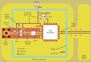
A well-designed GPS PCB Design should minimize electromagnetic interference (EMI), maintain stable power delivery, preserve RF signal integrity, and provide adequate mechanical and environmental protection.
For applications such as vehicle tracking, fleet management, navigation systems, drones, industrial IoT, asset tracking, and wearable devices, careful PCB engineering is essential to maintain stable satellite reception under real-world conditions.
For manufacturers such as Kingda, integrating RF considerations into PCB Design, PCB fabrication, and PCBA Manufacturing can help customers move from prototype validation to reliable mass production.
Key Takeaways
- Select the GPS module according to application requirements, including size, power consumption, sensitivity, positioning accuracy, interfaces, and operating temperature.
- Carefully plan GPS Antenna placement and maintain an appropriate antenna keep-out area.
- Use a continuous Ground Plane and a well-designed PCB stack-up to provide a stable RF return path.
- Keep RF traces short, direct, and impedance-controlled to minimize signal loss and unwanted reflections.
- Use appropriate power filtering, decoupling capacitors, LDO regulators, and protection components to maintain a clean supply.
- Separate sensitive GPS circuitry from noisy digital interfaces, switching regulators, motors, and other EMI sources.
- Validate the prototype in the actual operating environment before moving to mass production.
- Work with an experienced PCB Manufacturing partner to control fabrication tolerances, RF characteristics, assembly quality, and production consistency.
GPS Module Selection
Selecting the right GPS module is the first step in developing a reliable GPS-based product. The module should match the application’s electrical, mechanical, RF, and environmental requirements.
Application Requirements
Start by defining how the GPS system will be used.
A vehicle tracking device may require a compact module with low power consumption, fast positioning, strong sensitivity, and reliable performance under vibration and temperature changes.
Navigation equipment may prioritize positioning accuracy and fast time-to-first-fix (TTFF), while industrial tracking equipment may require extended temperature operation, long-term availability, and robust interfaces.
Important selection criteria include:
- Module dimensions.
- Operating voltage.
- Power consumption.
- Receiver sensitivity.
- Positioning accuracy.
- Cold-start and hot-start performance.
- Communication interfaces.
- Supported satellite constellations.
- Antenna compatibility.
- Operating temperature.
- Firmware and configuration options.
Before comparing modules, clearly define the primary application requirements. This prevents unnecessary specifications from influencing the selection process.
Module Features
A typical GPS module specification may include parameters such as:
| Parameter | Typical Consideration |
|---|---|
| Module size | Determined by product enclosure and PCB area |
| Supply voltage | Commonly 3.3 V or 5 V depending on module |
| Communication | UART, USB, I²C, SPI, or other interfaces |
| Receiver sensitivity | Important for weak-signal environments |
| Positioning accuracy | Depends on receiver, antenna, environment, and correction technology |
| Time to first fix | Influenced by satellite visibility and startup conditions |
| Antenna interface | Passive or active antenna support |
| Satellite systems | GPS, Galileo, GLONASS, BeiDou, or multi-constellation support |
| Operating temperature | Must match the target application |
| Applications | Tracking, navigation, logistics, IoT, drones, and industrial systems |
The final specifications should always be verified against the selected module’s current datasheet rather than relying on generic values.
You should also evaluate grounding, shielding, RF routing, and antenna compatibility during module selection. A high-performance receiver cannot compensate for poor PCB implementation.
Environmental Considerations
The operating environment can significantly influence GPS PCB reliability.
Outdoor equipment may be exposed to:
- Dust.
- Moisture.
- Rain.
- Condensation.
- UV exposure.
- Temperature cycling.
- Mechanical vibration.
- Shock.
- Corrosive contaminants.
High temperatures can accelerate component aging, increase leakage currents, affect oscillator stability, and reduce the reliability of solder joints and electronic components.
Moisture can contribute to corrosion, leakage paths, and electrical shorts. For industrial applications, the enclosure, conformal coating, connectors, and PCB material should therefore be evaluated together.
When selecting a GPS module, verify its operating and storage temperature ratings and make sure they are compatible with the final product environment.
PCB Design: Schematic Essentials
A robust GPS PCB Design starts with a well-structured schematic.
The schematic should clearly define:
- GPS module power input.
- Ground connections.
- RF antenna interface.
- Communication interfaces.
- Reset and enable signals.
- Backup power.
- Oscillator or reference clock requirements.
- Protection circuitry.
- Filtering components.
- Status indicators.
- Programming and debugging interfaces.
A clear schematic also simplifies troubleshooting and manufacturing documentation.
Supporting Components
GPS modules typically require supporting components for stable operation.
Depending on the module architecture, these may include:
- Decoupling capacitors.
- Bulk capacitors.
- Ferrite beads.
- Voltage regulators.
- Resistors.
- Crystals or oscillators.
- ESD protection devices.
- TVS diodes.
- RF matching components.
- Antenna connectors.
Component values should be selected according to the GPS module manufacturer’s reference design and datasheet.
Place critical passive components close to the corresponding module pins. Excessive trace length between the module and its decoupling or filtering components can reduce their effectiveness.
For RF circuits, the manufacturer’s recommended layout should be treated as a starting point rather than simply copied without considering the complete PCB stack-up and antenna environment.
Power and Data Connections
Power and data routing require careful planning because switching noise from digital circuits can interfere with sensitive GPS reception.
Recommended practices include:
- Keep GPS power connections short.
- Separate noisy switching power circuits from the RF section.
- Use appropriate trace widths based on current requirements.
- Keep high-speed digital interfaces away from the antenna and RF path.
- Route differential signals according to their interface requirements.
- Maintain appropriate impedance where required.
- Place decoupling capacitors close to power pins.
Power and data traces should be clearly identified in the schematic and PCB layout. This makes later debugging and design verification significantly easier.
Protection and Filtering
GPS electronics can be vulnerable to ESD, voltage transients, and conducted electrical noise.
Protection components may include:
- TVS diodes.
- ESD suppressors.
- Ferrite beads.
- LC filters.
- Decoupling capacitors.
- Overvoltage protection.
- Reverse-polarity protection.
The protection network should be designed so that it does not unnecessarily degrade the RF signal.
For example, ESD protection on an antenna input must have suitable RF characteristics and low parasitic capacitance.
GPS Module PCB Layout
PCB layout is one of the most critical stages of GPS product development.
A GPS receiver can have excellent specifications on paper but perform poorly if the antenna, RF trace, ground plane, power supply, and noisy circuits are improperly arranged.
Antenna Placement
The GPS Antenna is one of the most sensitive components in the entire system.
The antenna location should be determined early in the PCB design process rather than treated as an afterthought.
For ceramic patch antennas, the antenna may require a large ground structure and sufficient clearance depending on the manufacturer’s recommended layout.
For chip antennas and other compact antennas, placement at the PCB edge is often advantageous because it provides a more open electromagnetic environment.
Important antenna-layout considerations include:
- Follow the antenna manufacturer’s recommended keep-out area.
- Keep metal objects away from sensitive antenna regions.
- Avoid routing high-speed digital signals underneath or immediately beside the antenna where prohibited by the antenna design.
- Keep batteries and large metal components away from the antenna.
- Maintain an appropriate ground structure.
- Keep the RF feed line short.
- Avoid unnecessary vias in the RF path.
- Provide an impedance-controlled RF transmission line.
The required clearance is application- and antenna-dependent. A fixed distance such as 20 mm should not be treated as a universal rule; always follow the antenna vendor’s layout recommendations and validate the design experimentally.
Design Tip: Mark the antenna keep-out area directly in the PCB layout database so that copper, components, vias, and mechanical structures are not accidentally placed in restricted areas.
PCB Stack-Up
The PCB stack-up has a direct influence on RF performance and signal integrity.
A suitable multilayer stack-up can provide:
- A continuous reference plane.
- Controlled impedance.
- Short return-current paths.
- Better electromagnetic shielding.
- Improved power distribution.
- Better mechanical rigidity.
For a multilayer GPS board, a common approach is to place RF traces on an outer layer with a continuous reference plane immediately below them.
Sensitive analog and RF circuitry should be physically separated from noisy digital and power circuitry.
The exact layer arrangement depends on board thickness, dielectric material, controlled impedance requirements, manufacturing capability, and antenna architecture.
Special structures such as blind vias or back-drilled vias may be useful in high-density designs, but they should only be used when they provide a clear electrical or mechanical benefit.
Routing and Signal Integrity
RF routing must be carefully controlled.
The RF PCB Layout should generally use short, direct traces with controlled impedance.
Recommended practices include:
- Keep RF traces as short as practical.
- Maintain a continuous reference ground beneath the RF transmission line.
- Avoid unnecessary bends.
- Use smooth routing where bends are unavoidable.
- Avoid abrupt changes in trace width.
- Minimize unnecessary vias.
- Keep noisy digital signals away from the RF path.
- Place matching components close to the RF interface.
- Follow the impedance requirements specified by the GPS module or antenna manufacturer.
The RF transmission line should be designed according to the actual PCB stack-up. Trace width alone does not determine impedance; dielectric thickness, dielectric constant, copper thickness, trace geometry, and reference-plane configuration all matter.
A professional PCB manufacturer such as Kingda can help verify stack-up and impedance requirements before fabrication.
Power and Grounding
Clean Power Design
GPS receivers are sensitive to power-supply noise.
Switching regulators, DC-DC converters, processors, displays, motors, and high-speed interfaces can introduce conducted and radiated noise into the GPS receiver.
Where appropriate, an LDO can be used after a switching regulator to provide a lower-noise supply for sensitive RF circuitry.
A good power architecture may include:
- A stable primary power source.
- Appropriate voltage regulation.
- Local decoupling.
- Ferrite filtering.
- Bulk capacitance.
- Proper power-plane design.
- Protection against voltage transients.
The selected regulator must meet the GPS module’s voltage, current, noise, transient-response, and thermal requirements.
Power components that generate substantial switching noise should be physically separated from the GPS receiver and antenna.
Ground Plane Strategy
A continuous Ground Plane is essential for many GPS and RF PCB designs.
The ground plane provides a low-impedance return path and can reduce unwanted electromagnetic radiation.
Recommended practices include:
- Maintain continuous reference ground under RF traces.
- Avoid unnecessary gaps beneath sensitive RF routing.
- Use sufficient ground vias around RF structures where appropriate.
- Connect shielding structures to a low-impedance ground.
- Avoid creating unintended return-current paths through noisy circuitry.
Ground-plane design should be considered together with the PCB stack-up and RF transmission-line geometry.
Decoupling
Decoupling capacitors help stabilize the supply voltage and reduce high-frequency power noise.
Typical strategies include:
- Placing small-value high-frequency capacitors close to the module power pins.
- Adding larger capacitors for lower-frequency load variations.
- Minimizing the loop area between the power pin, capacitor, and ground.
- Using the component values recommended by the module manufacturer.
A 100 nF capacitor is commonly used for high-frequency decoupling, but it should not be considered a universal value. The complete decoupling network should be designed according to the module’s power requirements and measured noise characteristics.
Good decoupling can improve power integrity and help the final product pass EMC testing.
Antenna Integration and EMI Suppression
Antenna Selection
The antenna has a major influence on GPS reception performance.
Common antenna types include:
Active Antennas
Active antennas integrate a low-noise amplifier (LNA). They can improve system sensitivity when the antenna is connected through a longer cable or operates in a challenging RF environment.
However, they require an appropriate DC bias supply and filtering network.
Passive Antennas
Passive antennas do not contain an integrated amplifier. They generally have a simpler electrical architecture and can provide excellent performance when placed in a suitable RF environment.
Ceramic Patch Antennas
Patch antennas are widely used in navigation and tracking equipment. Their performance depends strongly on ground-plane size, orientation, placement, and surrounding materials.
Chip Antennas
Chip antennas offer compact dimensions and can be useful in space-constrained products. Their performance is highly dependent on the PCB layout and antenna keep-out region.
External Antennas
External antennas can provide greater flexibility when the GPS receiver needs to be positioned away from the main electronics or installed inside a vehicle, industrial cabinet, or other enclosure.
The antenna should always be selected together with the enclosure, PCB dimensions, ground plane, and target operating environment.
Antenna Matching and Tuning
A matching network allows the antenna system to be optimized for the actual PCB and enclosure environment.
A typical matching network may use:
- Capacitors.
- Inductors.
- Transmission-line structures.
- RF connectors.
- Optional filter components.
A vector network analyzer (VNA) can be used to evaluate antenna impedance and return loss.
If the antenna type, PCB stack-up, enclosure, ground-plane dimensions, or antenna location changes significantly, the matching network may need to be reevaluated.
The antenna manufacturer’s reference design should always be used as the starting point.
EMI Mitigation
Electromagnetic interference can significantly reduce GPS receiver performance.
Potential noise sources include:
| EMI Source | Typical Mechanism |
| Digital clocks | High-frequency harmonics |
| Switching ICs | Rapid voltage and current transitions |
| DC-DC converters | Switching noise and harmonics |
| LED drivers | Wideband switching noise |
| Motor controllers | Rapid current changes |
| Motors | Magnetic-field and commutation noise |
| USB 3.x interfaces | High-frequency broadband emissions |
| Long high-speed cables | Radiated and conducted interference |
| Unshielded cables | Uncontrolled RF coupling |
To reduce EMI:
- Keep the GPS receiver and antenna away from noisy circuits.
- Use a continuous ground reference.
- Keep high-speed digital traces away from the RF section.
- Use suitable shielding where required.
- Add ferrite beads and filtering components where appropriate.
- Keep power and data connections short.
- Avoid routing high-speed signals near the antenna.
- Verify the design through EMC and RF testing.
EMI mitigation should be evaluated at the system level because interference can enter through the antenna, power supply, digital interfaces, cables, enclosure, or PCB itself.
Prototype Development and Testing
A prototype provides the first opportunity to verify whether the theoretical PCB design performs correctly in the real world.
Assembly
Before assembly, verify the PCB fabrication data, component specifications, polarity, footprints, and assembly drawings.
During prototype assembly:
- Inspect the PCB for fabrication defects.
- Verify component orientation.
- Follow the recommended soldering profile.
- Use appropriate ESD protection.
- Inspect solder joints.
- Verify RF connectors.
- Check for shorts and open circuits.
- Clean flux residues when required.
- Perform electrical inspection before powering the board.
For production-level development, automated optical inspection (AOI) and automated electrical testing can improve consistency and traceability.
GPS Performance Testing
After assembly, connect the GPS PCB to a controlled power source and verify the communication interface.
Testing should evaluate parameters such as:
- Time to first fix.
- Positioning accuracy.
- Satellite count.
- Carrier-to-noise density ratio (C/N₀).
- Receiver sensitivity.
- Update rate.
- Power consumption.
- Cold-start performance.
- Hot-start performance.
- Position stability.
Testing should be performed in both controlled and representative real-world environments.
For example, a GPS tracker intended for vehicles should be tested inside the target enclosure and near the actual power electronics rather than only on an open laboratory bench.
Test results should be recorded and compared against the design requirements.
Troubleshooting
Common prototype problems include:
- Weak GPS signal.
- Long time to first fix.
- Unstable positioning.
- Excessive noise.
- Incorrect antenna matching.
- Poor solder joints.
- Power-supply noise.
- RF routing problems.
- Inadequate ground reference.
- EMI from digital interfaces.
A structured troubleshooting process should begin with power and ground verification, followed by communication, antenna, RF routing, and environmental checks.
| Issue | Possible Cause | Recommended Investigation |
| Weak GPS signal | Poor antenna placement | Check antenna orientation and keep-out area |
| High RF loss | Incorrect RF routing | Verify impedance and trace geometry |
| Position instability | EMI or poor antenna environment | Test with noisy circuits disabled |
| Power instability | Regulator or decoupling problem | Measure supply ripple |
| Soldering failure | Incorrect assembly process | Inspect solder joints and footprints |
| Short circuit | Manufacturing defect | Perform electrical inspection |
| Thermal problem | Excessive component dissipation | Measure temperature distribution |
| Poor sensitivity | Antenna mismatch | Measure antenna return loss |
PCB Manufacturing Considerations for GPS Products
A technically correct design can still fail during mass production if the PCB manufacturing process is not sufficiently controlled.
For GPS applications, manufacturing considerations may include:
- PCB layer alignment.
- Controlled dielectric thickness.
- Copper thickness.
- RF trace geometry.
- Impedance control.
- Via dimensions.
- Solder-mask registration.
- Surface finish.
- Component placement accuracy.
- Assembly quality.
- Cleanliness.
For RF-sensitive boards, even small changes in stack-up or trace geometry can affect impedance.
Therefore, the PCB manufacturer should receive complete fabrication requirements, including the required stack-up, material specifications, impedance targets, copper thickness, and tolerance requirements.
For high-volume production, process control should also include inspection of solder joints, component placement, vias, connectors, and RF interfaces.
Kingda can support customers by integrating PCB fabrication and PCBA considerations into the product-development process, helping engineers move from prototype boards toward stable mass production.
Common GPS PCB Design Failure Points
Several recurring problems can reduce GPS PCB reliability.
| Failure Point | Typical Problem | Design Countermeasure |
| Environmental exposure | Moisture, dust, corrosion | Appropriate enclosure and protection |
| Thermal stress | Component aging and solder degradation | Thermal design and testing |
| Aging components | Capacitor or component degradation | Qualified components and lifecycle management |
| RF interference | Weak or unstable GPS signal | Proper antenna placement and EMI control |
| Poor grounding | Increased noise | Continuous ground plane |
| Incorrect antenna matching | RF power loss | VNA-based tuning |
| Poor PCB fabrication | Impedance or dimensional variation | Controlled manufacturing |
| Assembly defects | Open or short circuits | AOI and electrical testing |
Systematic design reviews and manufacturing controls can prevent many of these problems before they become expensive field failures.
Best Practices for Reliable GPS PCB Design
A reliable GPS PCB should be developed around several core principles:
1. Follow the Module Reference Design
The GPS manufacturer’s reference circuit and layout recommendations provide an important starting point.
However, the final design must also account for the actual PCB stack-up, enclosure, antenna, power architecture, and surrounding electronics.
2. Protect the RF Section
Keep the antenna and RF path away from noisy digital and power circuits.
3. Maintain a Stable Ground Reference
A continuous ground plane provides a predictable return-current path and supports RF signal integrity.
4. Control the Power Supply
Use appropriate regulators, filters, and decoupling networks to minimize supply noise.
5. Design for Manufacturing
Consider PCB fabrication tolerances, component availability, assembly processes, inspection, and testability from the beginning.
6. Validate Under Real Conditions
Laboratory testing is important, but the final product should also be tested inside its actual enclosure and under realistic environmental and electromagnetic conditions.
Frequently Asked Questions
What is the most important part of GPS module PCB design?
Antenna placement is one of the most critical factors. The antenna needs an appropriate electromagnetic environment, sufficient clearance, and a suitable ground structure.
However, antenna performance also depends on RF routing, grounding, matching, power integrity, enclosure design, and EMI control.
How can I reduce noise on a GPS PCB?
Use a continuous ground plane, clean power supply, appropriate decoupling, short RF traces, and physical separation between GPS circuitry and noisy digital or switching-power circuits.
High-speed interfaces should be kept away from the antenna and sensitive RF path.
Can any antenna be used with a GPS module?
No. The antenna must be electrically compatible with the GPS receiver and suitable for the required frequency bands and application.
The antenna type, gain, impedance, polarization, size, ground-plane requirements, and active/passive architecture should all be considered.
Why does a GPS module require a clean power supply?
GPS receivers process very weak satellite signals. Power-supply noise can couple into the RF and baseband sections and reduce receiver performance.
A properly designed regulator, filtering network, and decoupling strategy can help maintain stable operation.
Should the GPS antenna be tuned after PCB layout?
Yes. Antenna performance depends on the actual PCB, ground plane, enclosure, surrounding components, and installation environment.
After significant changes to the PCB or enclosure, antenna performance should be re-evaluated.
What PCB material should be used for GPS applications?
The material depends on the RF frequency, required dielectric characteristics, board cost, mechanical requirements, and manufacturing process.
For many standard GPS/GNSS products, conventional high-quality FR-4 can be sufficient when the RF layout is properly engineered. More specialized RF materials may be considered when tighter dielectric control or higher-frequency performance is required.
Conclusion
A reliable GPS Module PCB requires coordinated engineering across RF design, antenna integration, power management, grounding, signal routing, EMI suppression, PCB fabrication, assembly, and system testing.
The most important design areas include GPS PCB Design, GPS Antenna, RF PCB Layout, antenna keep-out, Ground Plane, controlled-impedance routing, clean power, and EMI mitigation.
The design should be validated through prototype testing before entering mass production. Manufacturing tolerances and PCBA processes must also be considered early so that the final product can maintain consistent RF performance from the first production batch to high-volume manufacturing.
For companies developing GPS trackers, navigation equipment, industrial IoT devices, automotive electronics, drones, or other satellite-positioning products, Kingda can be integrated into the PCB development and manufacturing workflow to support reliable PCB fabrication and PCBA production.