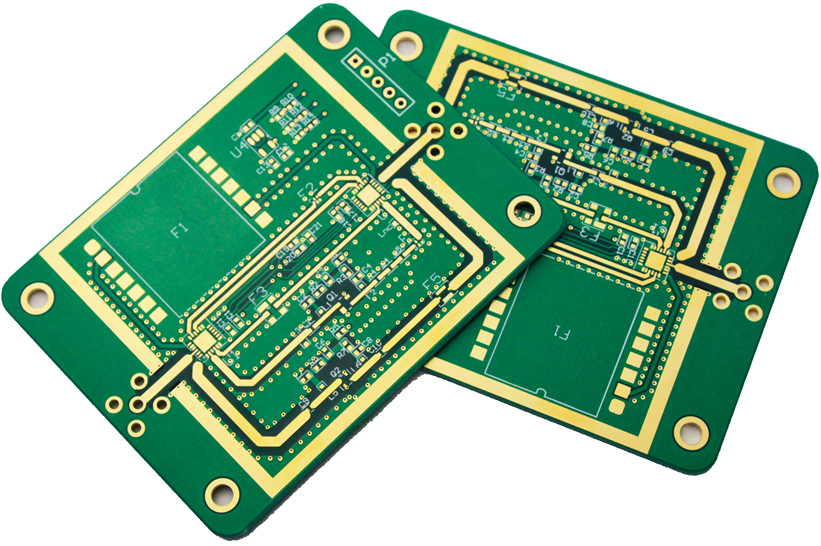
4 Layer PCB Manufacturer: Stackup and Fabrication Control
A four-layer board carries two outer signal layers and two inner layers for power, ground, or routing. The extra copper buys routing room, a steady reference plane, and better power delivery than a two-layer design. It also adds process steps that a fabricator must control: inner-layer imaging, lamination, drilling, plating, and impedance verification. Buyers comparing quotes often see the same layer count and assume the boards are equal. The real difference sits in stackup choices, material grades, and how tightly each step is recorded.
Most four-layer work starts with a stackup decision, not a price decision. The order of signal, ground, and power layers fixes impedance targets, return-current paths, and the dielectric thickness the drill and plating steps must respect. A fabricator who reviews your Gerber data and stackup drawing before tooling can flag problems early. That review costs little and prevents scrap later. When the stackup and the process plan agree, the first article has a fair chance of passing on the first build.
Stackup Choices That Matter
The signal-ground-power-signal arrangement is the workhorse for general digital and mixed-signal boards. Outer layers carry routing, while the inner ground plane gives high-speed traces a solid reference. The power plane sits below the ground plane and feeds the board through vias and pours. Because the signal-to-ground spacing controls trace width for a target impedance, the fabricator must hold that dielectric thickness within a stated window. Ask for the stackup drawing with nominal and tolerance values before you approve production.
A signal-ground-ground-signal stackup puts ground on both inner layers. This suits designs where crosstalk and emissions matter more than a dedicated power plane. Power then travels through wide traces or copper pours on the outer layers, which demands careful current planning. The payoff is strong shielding for sensitive traces and a stable reference on both sides. This choice fits communication, instrumentation, and positioning products where signal quality drives the design. Confirm that your power distribution still meets current and voltage-drop needs before committing.
Alternating signal and ground layers appear in noise-sensitive analog and high-speed work. Each signal layer references an adjacent ground plane, so return currents stay short and predictable. The tradeoff is awkward power distribution, since no layer is set aside for supply rails. Engineers sometimes accept that cost when shielding and impedance stability dominate. A fabricator should review the design against this stackup before quoting, because the routing density and via count change the drilling and plating load.
Two internal power layers suit boards with several voltage rails. Each inner layer can serve a different supply, while the outer layers handle signals. Ground then comes from pours or local areas on the signal layers, which needs attention to continuity. This stackup works when the rail count and current demand justify the lost routing space. The right answer depends on voltage domains, current draw, signal speed, and the overall board architecture. Bring those numbers to the fabricator early, so the stackup review is grounded in real requirements.
How to Judge a Fabricator
Start with the questions a supplier can answer in writing. Ask which stackups they build routinely, which material grades they stock, and how they verify impedance on a production lot. A serious partner will show a stackup drawing, a process flow, and a test plan rather than a price alone. Ask how they handle engineering questions raised during file review. A supplier that answers before tooling is cheaper than one that guesses and rebuilds. Our quality management approach records these checks with each lot.
Material choice drives both performance and cost. Standard FR-4 covers most general-purpose four-layer boards, and high-Tg grades help where thermal cycling is expected. Low-loss laminates enter the picture when frequency and loss budgets demand them. Each grade carries its own dielectric constant, dissipation factor, and thermal limits, so the stackup must be recalculated when the material changes. Do not assume a stackup built for one laminate transfers unchanged to another. Ask the fabricator to confirm impedance targets against the actual material lot.
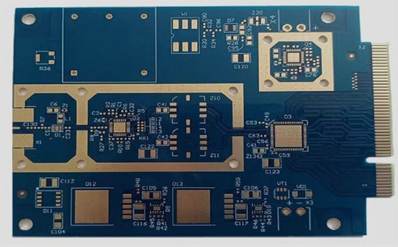
Copper weight is another decision buyers often leave to default. Heavier copper helps current capacity and heat spreading, but it complicates etching and plating. Thin copper keeps fine traces sharp but limits current. The right value follows from current density, thermal needs, and trace geometry, not from a habit of maximizing thickness. Surface finish follows the same logic. HASL suits many through-hole assemblies, while ENIG helps fine-pitch parts and long shelf life. Each finish has process limits the fabricator should state clearly.
Fabrication Steps Under Control
Inner-layer imaging and etching set the pattern that lamination will bury. Trace width, spacing, and registration are checked after etch, because errors here cannot be corrected later. Lamination then bonds the cores and prepreg under controlled heat, pressure, and time. Poor lamination shows up as voids, delamination, or thickness variation, and those faults surface at test or in the field. A fabricator should record lamination parameters per lot and keep them with the build record. That record answers questions months later when a field return arrives.
Drilling comes next, and it carries real risk in four-layer work. Hole position, diameter, and wall quality decide whether plating forms a reliable barrel. Smear left in the hole blocks the copper-to-copper connection, so desmear control matters. Standard through-holes are routine, while blind, buried, and microvia structures add steps and cost. Buyers should match the drilling spec to the design rather than to a template. If your design needs advanced vias, confirm the fabricator builds them before you release the files for tooling.
Plating thickness and uniformity determine long-term reliability. Thin barrel plating can crack under thermal cycling, and uneven plating narrows the process window at assembly. Outer-layer imaging and etching then define the surface pattern, with registration checked against the drilled holes. Solder mask protects exposed copper and reduces bridging during assembly. Silkscreen marks references and polarity for the assembly team. Each step feeds the next, so a drift in one area appears as a defect in another.
That is why process data should be reviewed as a chain, not as isolated operations. For the surface-mount stage that follows, see our SMT PCB assembly notes.
Cost Drivers and Tradeoffs
Board size and quantity shape panel utilization and setup cost. Larger boards use more material, and small lots spread the same setup over fewer units. Material grade moves the price quickly when low-loss or high-Tg laminates replace standard FR-4. Copper weight adds material and process time. Controlled impedance adds engineering and test steps that are worth paying for on high-speed designs. Advanced drilling adds steps that a standard through-hole board never needs. A quote that lists these items separately helps you compare suppliers on equal terms.
Testing is where many buyers cut too deep. Automated optical inspection catches pattern and mask faults, and electrical test confirms connectivity. Neither proves the board works under power. For assembled boards, PCBA testing adds in-circuit and functional checks that catch wrong parts and weak joints. A four-layer board with controlled impedance may also need coupon measurement to confirm the stackup held during lamination. Ask which tests run on every lot and which run only on the first article. The answer tells you how much confidence the price includes.
Choosing Between Two and Four Layers
A two-layer board remains the economical choice for simple circuits with moderate routing and no strict impedance needs. Four layers earn their cost when routing density rises, when a solid reference plane is needed, or when power distribution must stay quiet. The added cost buys design margin, and that margin often removes rework and respins. Compare the total project cost, not the bare board price.
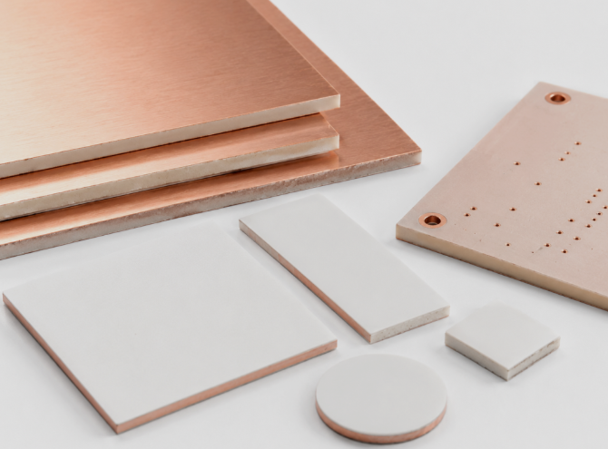
A board that needs fewer revisions and assembles with fewer defects can be cheaper overall even at a higher unit price. Document the reason for the layer count so the decision survives a design review.
Typical four-layer users include industrial controls, embedded computing, networking gear, and mixed-signal instruments. Automotive and medical products enter the list when reliability and traceability requirements are met. The final call rests on frequency, current, mechanical limits, and production volume. If your design also needs assembly, keeping fabrication and PCB assembly with one supplier reduces handoffs and shortens the feedback loop. A single partner sees the bare board data and the placement data together, which makes defect tracing faster when something goes wrong.
Prototype Before Volume
Prototypes are the cheapest place to find mistakes. A small pilot lot reveals pad geometry issues, material behavior, and process limits before volume commitment. Use rapid PCBA prototyping to test the stackup and assembly together, so impedance and solderability are proven on real boards. Record the settings used on that build. Those settings become the baseline for the production lot, and any later change can be compared against them. Buyers who invest in this stage usually reach volume with fewer surprises and a shorter schedule.
When the design moves to volume, the same discipline applies at higher stakes. Ask for first-article approval with measured impedance, plating thickness, and hole quality. Review the inspection plan and the test coverage before release. Confirm how the fabricator handles material substitutions and whether you will be notified. A written change process protects both sides when a laminate or finish becomes unavailable. These steps cost little at the start and prevent expensive surprises later. The goal is a repeatable board, not a lucky batch.
What to Verify Before Ordering
Send complete data: Gerbers, drill files, stackup drawing, impedance targets, copper weight, board thickness, surface finish, and quantity. State which tests you require and which standards apply. Ask for the stackup in writing with nominal values and tolerances. Confirm lead time after file review, not before, because material availability and drilling complexity change the schedule. A fabricator that answers these points clearly is easier to hold to a delivery date. Clear input at the start removes most disputes at the end of the run.
The practical takeaway is simple. Treat the stackup as an engineering document and the process record as part of the product. Ask your fabricator to show both before you place the order. Compare quotes on the same stackup, material, finish, and test scope, so the numbers mean something. Then check the first article against the drawing and keep the results with the lot. A four-layer board is only as good as the control behind it, and that control is visible in the paperwork long before it shows on the bench.