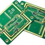
6-Layer PCB Manufacturer
High-quality 6-layer PCB solutions provide an effective balance between routing density, electrical performance, manufacturing complexity, and cost. As electronic products become smaller and more sophisticated, designers increasingly require additional PCB layers to accommodate high-speed signals, power distribution, grounding, and complex component interconnections.
A six-layer board provides four internal copper layers in addition to the top and bottom layers. This additional routing space makes it possible to develop more sophisticated circuit architectures while maintaining controlled impedance, reliable signal-return paths, and improved electromagnetic compatibility.
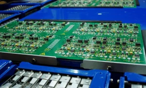
For demanding projects, professional 6-layer PCB manufacturing requires careful control of materials, lamination, drilling, copper plating, impedance, registration, and electrical testing. A suitable manufacturing partner should also provide engineering support and DFM analysis before fabrication.
For broader manufacturing requirements, see our PCB Manufacturing capabilities.
What Is a 6-Layer PCB?
A 6-layer PCB contains six conductive copper layers separated by dielectric insulating materials. Depending on the electrical and mechanical requirements of the product, these copper layers can be assigned as signal layers, ground planes, or power planes.
A common six-layer structure may use:
- Layer 1 – Signal / Components
- Layer 2 – Ground
- Layer 3 – Signal / Power
- Layer 4 – Power / Signal
- Layer 5 – Ground
- Layer 6 – Signal / Components
The exact structure should not be selected simply because it is commonly used. The optimum 6-layer PCB stackup depends on signal speed, impedance requirements, power distribution, thermal requirements, component density, PCB thickness, material selection, and manufacturing capabilities.
Six-layer boards can also incorporate advanced technologies such as blind vias, buried vias, microvias, HDI structures, controlled impedance, and specialized high-frequency materials when required.
Modern PCB manufacturers may support a broad range of multilayer structures, including high-TG, high-speed, high-frequency, HDI, rigid-flex, and heavy-copper technologies.
Why Choose a 6-Layer PCB?
Choosing between four, six, and eight PCB layers should be based on the actual electrical and mechanical requirements of the product.
A four-layer board may become difficult to route when the design contains numerous high-speed interfaces, multiple power domains, dense BGA packages, or strict EMC requirements. Adding two additional copper layers can provide the routing and reference-plane space needed to solve these challenges.
A six-layer structure is often attractive because it offers more design flexibility than a four-layer board without introducing the additional cost and complexity of an eight-layer or higher-layer-count construction.
The main reasons to select a six-layer design include:
- Increased routing capacity
- Better ground-plane distribution
- Improved signal-return paths
- More effective power distribution
- Better electromagnetic compatibility
- Higher component density
- Improved controlled-impedance routing
- Greater flexibility in stackup design
- Support for more complex electronic systems
A properly engineered multilayer PCB can also separate sensitive signals from noisy power or digital circuits, helping engineers manage signal integrity and electromagnetic interference.
Advantages of 6-Layer PCB Manufacturing
Improved Signal Integrity
One of the most important benefits of a 6-layer PCB is improved signal integrity.
Additional reference planes allow high-speed traces to be routed close to continuous ground or power-reference structures. This can create more predictable impedance and shorter return paths.
For high-speed interfaces, the stackup should be designed before routing begins. Trace width, dielectric thickness, copper thickness, and dielectric properties all influence the final impedance.
Professional PCB design services can assist with stackup development, impedance calculations, EMC considerations, and manufacturability. See our PCB Design & Layout Services for related engineering capabilities.
Better EMC Performance
Electromagnetic compatibility is another important reason to use six layers.
Ground planes can provide shielding between signal layers and help establish controlled return-current paths. Sensitive signals can also be routed between reference planes to reduce unwanted electromagnetic coupling.
However, simply adding more PCB layers does not automatically guarantee better EMC performance. The layer arrangement, plane continuity, via transitions, component placement, routing strategy, and return-current paths must all be considered during design.
Higher Routing Density
Additional internal layers create significantly more routing space.
This is particularly useful for boards containing:
- High-pin-count processors
- BGA packages
- Memory devices
- Multiple communication interfaces
- Power-management circuits
- Sensors
- Industrial controllers
- Automotive electronics
- Medical electronics
- Networking equipment
A well-designed six-layer board can provide considerably more routing flexibility while keeping the physical PCB relatively compact.
Flexible Layer Assignment
Six copper layers provide many possible combinations of signal, power, and ground planes.
Designers can assign layers according to application requirements instead of being restricted to a basic four-layer configuration.
For example, a design may prioritize:
- Two dedicated ground planes
- One or two power planes
- Multiple signal layers
- High-speed reference layers
- Specialized RF routing areas
This flexibility makes six-layer construction suitable for a wide range of advanced electronics.
Common 6-Layer PCB Stackup Configurations
The 6-layer PCB stackup is one of the most important decisions in the PCB development process. There is no universal stackup that is ideal for every application.
SIG – GND – PWR – PWR – GND – SIG
This symmetrical structure is suitable for designs requiring controlled high-speed routing and effective reference planes.
The top and bottom signal layers can use adjacent ground planes as references, while the internal power layers provide dedicated power distribution.
This arrangement can be useful for communication equipment, networking hardware, processors, and other systems containing multiple voltage domains.
SIG – GND – PWR – GND – SIG – GND
This configuration places ground planes next to most signal and power layers.
The strong ground reference can provide excellent shielding and power integrity. It can be useful for designs where EMI performance is particularly important.
However, the bottom layer being assigned to ground may reduce the available space for bottom-side component placement and routing.
SIG – PWR – SIG – SIG – GND – SIG
This structure provides a large amount of signal-routing space, but it may offer less effective electromagnetic shielding than configurations with more closely spaced ground references.
It may be appropriate for relatively low-speed or less EMI-sensitive designs, but it should not be selected for demanding high-speed applications without careful signal-integrity analysis.
SIG – GND – PWR – SIG – GND – SIG
This configuration provides ground references for multiple signal layers and can offer a better balance between routing capacity and EMC performance.
It is particularly useful for designs containing multiple high-speed interfaces and a relatively high I/O count.
The best stackup should always be developed according to the actual PCB design rather than copied from a generic template.
Key Design Considerations for a 6-Layer PCB
Successful 6-layer PCB manufacturing starts with a manufacturable design.
Layer Arrangement
Ground and power-plane placement has a direct impact on signal integrity, power integrity, and EMC.
High-speed traces should normally have a continuous reference plane nearby. Avoid routing signals across gaps or splits in their reference planes because this can force return currents to take longer paths and potentially increase EMI.
High-Speed Signal Routing
High-speed signals should be routed with careful attention to:
- Controlled impedance
- Trace geometry
- Reference planes
- Differential-pair spacing
- Via transitions
- Return-current paths
- Crosstalk
- Trace length
- Propagation delay
Where necessary, simulation and impedance calculations should be completed before final routing.
Thermal Management
As component density increases, thermal management becomes increasingly important.
Power devices, processors, regulators, and other heat-generating components can create localized thermal concentrations. Copper planes, thermal vias, appropriate copper thickness, and suitable PCB materials can help distribute heat.
The thermal design should be considered together with electrical and mechanical requirements rather than treated as a separate issue.
Core and Prepreg Selection
A six-layer board normally contains multiple dielectric structures consisting of cores and prepreg.
Dielectric thickness and material properties influence:
- Controlled impedance
- Signal propagation
- Crosstalk
- PCB thickness
- Lamination
- Mechanical stability
- Manufacturing cost
Material selection should therefore be based on electrical performance, thermal requirements, reliability, and production availability.
Materials Used for 6-Layer PCBs
Different applications require different PCB material systems.
Common choices include:
FR-4
Standard FR-4 remains one of the most widely used materials for general-purpose multilayer PCB applications.
It offers a practical balance between cost, mechanical strength, electrical performance, and manufacturability.
High-TG FR-4
High-TG materials provide improved thermal performance and are suitable for applications exposed to higher operating temperatures or demanding lead-free assembly processes.
High-Speed Materials
High-speed digital applications may require materials with more controlled dielectric characteristics and lower signal losses.
High-Frequency Materials
RF and microwave applications may require specialized materials such as Rogers-type laminates or other high-frequency systems.
Hybrid Material Structures
Some complex PCBs combine different dielectric materials within the same multilayer construction to balance cost and electrical performance.
Modern PCB manufacturing capabilities can support FR-4, high-TG, Rogers and other high-performance material systems depending on project requirements.
6-Layer PCB Manufacturing Process
A reliable 6-layer PCB manufacturer should maintain tight process control throughout fabrication.
A typical manufacturing sequence includes:
- Engineering review and DFM analysis
- Material preparation
- Inner-layer imaging
- Inner-layer etching
- Automated optical inspection
- Layer alignment and lamination
- Mechanical and laser drilling where required
- Through-hole copper plating
- Outer-layer imaging and etching
- Solder mask application
- Surface finishing
- Electrical testing
- Final inspection
- Packaging and shipment
Modern PCB fabrication processes may also include AOI, X-ray inspection, impedance testing, microvia inspection, and 100% electrical testing depending on the board structure and customer requirements.
Advanced Technologies for 6-Layer PCBs
Six-layer boards can support many advanced PCB technologies when the application requires them.
Blind and Buried Vias
Blind and buried vias can reduce routing congestion and provide more efficient layer-to-layer connections.
Microvias and HDI
When component pitch and routing density become especially challenging, HDI technology can provide smaller interconnections through laser-drilled microvias and sequential buildup structures.
For high-density applications, see our HDI PCB Manufacturing information.
Controlled Impedance
Controlled impedance is essential for many high-speed interfaces.
The PCB stackup, trace geometry, dielectric thickness, copper thickness, and material characteristics must be coordinated to achieve the required impedance.
High-Frequency PCB Technology
RF and microwave circuits may require specialized materials, controlled dielectric characteristics, and carefully engineered signal paths.
The appropriate material and stackup should be determined according to the operating frequency and electrical requirements.
Applications of 6-Layer PCBs
Six-layer boards are widely suitable for applications where a four-layer structure cannot provide enough routing space or electrical isolation.
Typical applications include:
- Industrial automation
- Robotics
- Telecommunications
- Networking equipment
- Medical electronics
- Automotive electronics
- Test and measurement equipment
- IoT devices
- Embedded computing
- Power-control systems
- Consumer electronics
- Aerospace electronics
The appropriate PCB construction depends on operating environment, circuit complexity, electrical performance, reliability requirements, and production volume.
6-Layer PCB vs. 4-Layer PCB vs. 8-Layer PCB
4-Layer PCB
A four-layer PCB is generally more economical and can be sufficient for moderate-complexity electronic products.
However, routing space may become limited when the design contains many high-speed signals, multiple power domains, or dense components.
6-Layer PCB
A 6-layer PCB provides a practical middle ground.
It adds two copper layers compared with a four-layer board, creating additional routing and reference-plane options without the complexity of a higher-layer-count design.
8-Layer PCB
An eight-layer board provides additional routing capacity and can be more appropriate for highly complex systems.
However, increased layer count generally means higher fabrication cost, more complicated lamination, and potentially longer manufacturing lead times.
Therefore, the correct choice should be based on the actual requirements rather than automatically selecting the highest layer count.
Quality Control for 6-Layer PCBs
Quality control is critical because multilayer PCB defects can exist inside the board and may not be visible during a conventional visual inspection.
Important inspection and testing methods include:
- Automated Optical Inspection (AOI)
- Electrical testing
- X-ray inspection
- Dimensional inspection
- Solder-mask inspection
- Copper thickness verification
- Layer-registration inspection
- Impedance testing
- Final visual inspection
For projects that require PCB assembly after fabrication, integrated manufacturing can reduce supplier coordination and simplify production management. Our PCB Assembly Services cover multilayer, HDI, rigid, flexible, rigid-flex, high-TG, high-frequency, and controlled-impedance PCB assembly requirements.
Cost Factors for 6-Layer PCBs
The price of a 6-layer PCB depends on much more than the number of layers.
Important cost factors include:
- Board dimensions
- Order quantity
- PCB thickness
- Copper weight
- Material selection
- Minimum trace and spacing
- Via structure
- Blind and buried vias
- Microvias
- Surface finish
- Controlled impedance requirements
- Special reliability requirements
- Testing requirements
- Production schedule
Specialized materials and advanced structures generally increase manufacturing costs.
For prototype and smaller production requirements, production planning and DFM optimization can also have a significant influence on the final unit price. Low-volume PCB production can be particularly useful during product development and engineering validation. See our Low-Volume PCB Assembly service for additional production support.
How to Choose a 6-Layer PCB Manufacturer
When selecting a 6-layer PCB manufacturer, evaluate more than the quoted price.
Consider the manufacturer’s:
- Multilayer PCB experience
- Material availability
- Layer-count capability
- HDI capability
- Impedance-control capability
- Drilling and plating technology
- Lamination control
- DFM engineering support
- Inspection and testing systems
- Quality certifications
- Prototype capability
- Production scalability
- Delivery performance
Engineering support is particularly important for complex six-layer boards. A manufacturer should be able to review the Gerber files, evaluate the stackup, identify manufacturability risks, and recommend improvements before fabrication.
Conclusion
A well-engineered 6-layer PCB can provide an excellent balance between routing density, signal integrity, EMC performance, component density, and manufacturing cost.
The most important step is not simply adding two more copper layers. The entire 6-layer PCB stackup must be engineered around the electrical, thermal, mechanical, and manufacturing requirements of the final product.
For demanding applications, designers should define the stackup early, establish controlled-impedance requirements, maintain continuous reference planes, evaluate thermal conditions, and confirm manufacturing capabilities before completing the PCB layout.
From prototype development to volume production, a professional 6-layer PCB manufacturer can provide the engineering expertise, fabrication technology, inspection processes, and production support needed to turn a complex PCB design into a reliable finished circuit board.
For projects requiring both PCB fabrication and downstream assembly, integrated PCB manufacturing and assembly can further simplify supplier management and improve production continuity.