PCB Via vs. Pad: Differences, Hole Tolerances, and Design Guidelines
When designing a printed circuit board, understanding the difference between a PCB Via and a PCB Pad is essential for achieving reliable electrical performance and smooth manufacturing. Although both can contain holes and connect to copper features, they serve different purposes in PCB construction.
A via is primarily designed to establish an electrical connection between different PCB layers, while a pad is designed to provide an electrical and mechanical connection for electronic components.
Understanding these differences can help engineers avoid manufacturing problems, improve assembly reliability, and optimize PCB layouts for production.
For complete PCB fabrication and assembly requirements, see our PCB Manufacturing Services.
What Is a PCB Via?
A PCB Via is a plated hole used to electrically connect copper traces, planes, or other conductive structures between different layers of a printed circuit board.
Depending on the PCB structure and design requirements, vias can generally be classified into:
- Through-hole vias
- Blind vias
- Buried vias
The primary purpose of a via is electrical interconnection between PCB layers. Unlike component mounting holes, vias are normally not intended for inserting and soldering component leads.
How Are Via Holes Used?
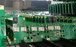
Vias provide vertical electrical paths through a multilayer PCB. For example, a signal routed on the top layer can use a via to transition to an internal routing layer.
Because vias are primarily electrical structures, their hole diameters do not necessarily require the same mechanical tolerance control as component mounting holes.
During PCB manufacturing, manufacturers may optimize via hole processing according to production conditions, available drill sizes, copper spacing, and surrounding design features.
For complex multilayer applications, understanding manufacturing capabilities before PCB fabrication is particularly important. Our PCB Assembly Services can support projects from prototype development through production.
Via Hole Size and Manufacturing Considerations
Via holes are often relatively small. Their final dimensions depend on factors such as:
- PCB layer count
- Board thickness
- Drill technology
- Minimum hole size
- Copper plating requirements
- Pad diameter
- Annular ring requirements
- Manufacturing tolerances
In dense PCB layouts, designers should avoid unnecessarily small vias unless they are required by electrical or mechanical constraints.
A smaller via can increase routing density, but it can also make fabrication more demanding. Therefore, the optimal via size should always consider both electrical requirements and the manufacturer’s process capabilities.
What Is a PCB Pad?
A PCB pad is a conductive copper area used to connect electronic components to the printed circuit board.
Pads can generally be divided into two major categories:
- Through-hole component pads
- Surface-mount pads
Through-hole pads contain holes that allow component leads to pass through the PCB. Surface-mount pads normally do not contain holes and are used to solder SMD components directly onto the PCB surface.
Unlike a via, a component pad provides both electrical connectivity and mechanical support.
For PCB projects requiring SMT, through-hole, or mixed assembly technologies, see our SMT PCB Assembly Services for more information.
PCB Via vs. Pad: Key Differences
The fundamental difference between a via and a pad is their intended function.
| Feature | PCB Via | PCB Pad |
|---|---|---|
| Primary purpose | Electrical connection between PCB layers | Component electrical and mechanical connection |
| Typical application | Layer-to-layer routing | Component soldering |
| Component lead insertion | Normally not used | Used for through-hole components |
| Hole tolerance | Generally less mechanically controlled | More strictly controlled |
| Mechanical function | Usually limited | Important for component mounting |
| Typical size | Often relatively small | Depends on component lead or package |
| Soldering function | Normally not required | Essential for component assembly |
In short, a via is primarily an interlayer electrical connection, while a pad is primarily a component connection point.
PCB Pad Hole Tolerance
Pad holes used for through-hole components require more precise dimensional control because the component lead must physically pass through the hole.
A hole that is too small can prevent component insertion. A hole that is excessively large can reduce the available annular ring and negatively affect soldering reliability or mechanical strength.
A practical design approach is to ensure that the finished hole is sufficiently larger than the maximum component lead dimension while maintaining an appropriate copper annular ring.
When selecting the hole diameter, engineers should consider:
- Maximum component lead size
- Lead shape
- Lead diagonal dimension for square or rectangular leads
- Finished-hole tolerance
- Plating thickness
- Component insertion requirements
- Soldering process
For example, if a component has a square lead, the diagonal dimension can be larger than the nominal side length. The PCB hole therefore needs to accommodate the actual maximum lead dimension rather than simply the nominal width.
Why Hole Tolerance Matters in PCB Manufacturing
Pad Hole Tolerance is particularly important for connectors, switches, terminal blocks, headers, and other through-hole components.
If the tolerance is too tight, the component may not fit correctly during assembly. If the hole is too large, the remaining copper around the hole may become insufficient.
For applications requiring controlled mechanical dimensions, engineers should clearly specify the required finished-hole tolerance in the PCB manufacturing documentation.
For projects that require PCB fabrication together with component sourcing and assembly, our Turnkey PCB Assembly service provides an integrated manufacturing approach.
Via Hole vs. Pad Hole: Manufacturing Differences
Although both vias and pads can contain plated holes, they are processed according to different design requirements.
Via Hole Manufacturing
Via holes are generally optimized for electrical interconnection and routing density. Their manufacturing requirements are strongly influenced by:
- PCB stackup
- Layer-to-layer connection requirements
- Drill diameter
- Aspect ratio
- Annular ring
- Copper plating
- High-density routing
In high-density PCB designs, designers may use blind or buried vias to reduce routing congestion and improve space utilization.
Pad Hole Manufacturing
Pad holes are primarily related to component assembly. Their design must account for:
- Component lead dimensions
- Finished-hole size
- Hole tolerance
- Soldering requirements
- Annular ring
- Component insertion
- Assembly process
Therefore, pad holes generally require more attention to mechanical fit than standard vias.
PCB Design Guidelines for Via and Pad Holes
Following practical PCB Design Guidelines can significantly reduce manufacturing and assembly risks.
1. Choose Via Sizes Based on Manufacturing Capability
Do not automatically use the smallest possible via. Smaller holes can increase fabrication complexity and may affect yield and cost.
The selected via size should be compatible with the PCB manufacturer’s standard process capability.
2. Use Appropriate Pad Hole Sizes
For through-hole components, the hole should be large enough to accommodate the maximum lead dimension while maintaining sufficient copper around the hole.
A small additional clearance is often useful to account for manufacturing tolerance and component variation.
3. Consider the Finished Hole Size
Engineers should distinguish between the designed drill size and the final plated hole size.
Copper plating changes the finished diameter, so PCB fabrication documentation should clearly define the required dimensions.
4. Consider the Annular Ring
The annular ring is the copper area surrounding a plated hole.
An insufficient annular ring can increase manufacturing risk and may affect PCB reliability, particularly when drilling accuracy, board thickness, and registration tolerances are taken into account.
5. Avoid Unnecessarily Small Vias
Small vias may be useful for BGA and high-density PCB routing, but they should only be used when required by the design.
For advanced BGA, HDI, and high-density designs, manufacturing feasibility should be reviewed before production.
Our PCBA Capabilities page provides additional information about PCB assembly technologies, component packages, and manufacturing capabilities.
Via and Pad Design for PCB Assembly

The distinction between vias and pads becomes especially important during PCB assembly.
During SMT assembly, component pads determine solder placement and component positioning. During through-hole assembly, plated pad holes must accommodate component leads and provide reliable solder joints.
For mixed-technology boards, designers need to consider both SMT and through-hole requirements simultaneously.
Our Mixed Technology PCB Assembly service supports assemblies combining surface-mount and through-hole components.
Common PCB Via and Pad Design Problems
Several common design mistakes can lead to PCB manufacturing or assembly problems.
Via Used as a Component Hole
A standard via should not normally be used as a substitute for a component mounting hole.
The dimensions, plating requirements, and mechanical function of the two structures are different.
Pad Hole Too Small
A hole that is smaller than the actual component lead can cause insertion problems or prevent automated assembly.
Always design according to the maximum component lead dimensions and manufacturing tolerance.
Pad Hole Too Large
An oversized hole reduces the copper surrounding the hole and may weaken the solder connection.
It can also make component positioning and soldering less reliable.
Insufficient Annular Ring
If the copper ring around a plated hole is too narrow, drill registration errors can result in breakout or reduced connection reliability.
Ignoring Manufacturing Capability
A design may be electrically correct but still difficult or expensive to manufacture.
Early DFM review can identify problematic hole sizes, spacing, annular rings, and other fabrication constraints before production.
How to Optimize PCB Designs for Manufacturing
Good PCB design is not only about electrical performance. Manufacturability should also be considered from the beginning of the design process.
Engineers should evaluate:
- Minimum drill diameter
- Finished-hole tolerance
- Pad diameter
- Annular ring
- Hole-to-hole spacing
- Hole-to-copper clearance
- Board thickness
- Aspect ratio
- Component lead dimensions
- SMT and THT assembly requirements
A professional DFM review can identify potential manufacturing issues before PCB fabrication and assembly.
For rapid prototype projects, our Rapid PCBA Prototyping service supports PCB assembly from prototype development through short-run production.
Conclusion
Understanding the difference between a PCB Via and a PCB Pad is fundamental to reliable PCB design and manufacturing.
A via is primarily used to create electrical connections between different PCB layers, while a pad provides an electrical and mechanical interface for component assembly. Their hole sizes, tolerances, annular rings, and manufacturing requirements should therefore be designed according to their specific functions.
For reliable PCB production, engineers should consider both electrical requirements and manufacturing capabilities when selecting via and pad dimensions.
By applying practical PCB Design Guidelines, using appropriate Via Hole structures, and carefully controlling Pad Hole Tolerance, designers can reduce manufacturing risks, improve assembly efficiency, and achieve more reliable electronic products.
If you are developing a new PCB or PCBA project, GOPCBA provides integrated PCB fabrication, component sourcing, SMT/THT assembly, testing, and turnkey manufacturing solutions. Visit our Contact Us page to discuss your project requirements with our engineering team.