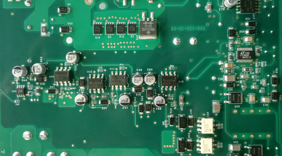
PCB Solder Mask Design Basics
For a typical double-sided PCB, the structure extending from the substrate toward both sides generally consists of copper circuit layers, solder mask layers, and silkscreen layers. Plated holes and vias provide electrical connections between the top and bottom copper layers.
A properly designed PCB solder mask plays an important role in protecting copper traces, preventing accidental soldering, and improving the reliability of the finished circuit board.
For projects that require both PCB fabrication and assembly, it is also important to consider solder mask design together with PCB assembly requirements. GOPCBA provides integrated PCB manufacturing and assembly services, helping engineers evaluate manufacturability before production.
What Is the Purpose of Solder Mask?
Solder mask, sometimes called solder resist, is the protective coating applied to selected areas of a printed circuit board. It performs several important functions during PCB manufacturing and assembly.
1. Protects Copper From Moisture and Chemicals

Solder mask helps protect exposed copper from moisture, contaminants, and chemical electrolytes that could otherwise accelerate oxidation and corrosion.
This protection helps maintain stable electrical performance and improves the long-term reliability of the PCB.
2. Prevents Mechanical Damage and Short Circuits
The solder mask provides an insulating protective layer over most of the copper circuitry.
It helps prevent accidental contact between conductive areas and reduces the possibility of short circuits caused by mechanical scratches or conductive contamination.
3. Prevents Unwanted Solder Connections
During PCB assembly, solder should only be applied to designated solder pads.
A properly designed solder mask opening exposes the required copper pads while keeping surrounding traces and copper areas covered. This helps prevent solder bridges and unintended electrical connections between adjacent components.
For complete PCB fabrication and assembly requirements, engineers can also review GOPCBA’s PCB Manufacturing Services.
4. Reduces Surface-Finish Consumption
Solder mask limits the amount of copper that needs to receive a surface finish such as HASL or ENIG.
Only designated exposed copper areas generally require the selected surface finish, helping reduce unnecessary processing and material consumption.
5. Improves PCB Appearance
Solder mask is available in different colors, including green, black, blue, red, and other options depending on manufacturing capabilities.
In addition to protecting the PCB, the coating also provides a consistent visual appearance for the finished product.
Understanding PCB Solder Mask Design
The term “solder mask” can sometimes cause confusion for engineers who are new to PCB design.
Solder mask does not simply mean “areas where solder is prohibited.” Instead, the solder mask layer defines the areas where the protective coating should be removed to expose copper.
In common PCB CAD and Gerber terminology, the Solder Mask layer is typically treated as a negative layer.
This means:
- Areas containing solder mask openings represent locations where solder mask is removed.
- Areas without openings remain covered by solder mask.
- When a solder mask opening overlaps a copper pad, the underlying copper becomes exposed.
Therefore, the relationship between the copper layer and solder mask layer determines the final exposed pad geometry.
Three Basic Rules for Solder Mask Design
Rule 1: Copper Layer Geometry Defines the Copper Area
The copper layer determines where conductive copper is manufactured.
Copper traces, pads, planes, and other conductive structures are created according to the corresponding PCB fabrication data.
Rule 2: Solder Mask Openings Expose Copper
A solder mask opening defines an area where solder mask is removed.
The exposed region can then receive solder during assembly or a surface finish during PCB fabrication.
Rule 3: Overlapping Copper and Solder Mask Openings Create Exposed Copper
The final exposed area is determined by the relationship between the copper geometry and the solder mask opening.
For example, if the solder mask opening is slightly larger than a copper pad, the exposed copper area is still limited by the actual copper geometry.
This is why PCB pad design and solder mask design should be considered together rather than independently.
How Is Solder Mask Manufactured?
After the copper circuitry has been formed, the PCB enters the solder mask production stage.
The basic process typically includes surface preparation, solder mask application, exposure, development, curing, and subsequent surface finishing.
Step 1: Copper Surface Preparation
After circuit etching, the copper surface is cleaned and treated.
Oxides, contaminants, and other residues are removed, while the copper surface may be roughened to improve adhesion between the copper and solder mask material.
Proper surface preparation is important because poor adhesion can lead to solder mask peeling or other manufacturing defects.
Step 2: Solder Mask Application
Solder mask ink is applied across the PCB surface.
The board is then dried or partially cured before the imaging process.
Depending on the manufacturing process, solder mask may be applied using different coating and imaging technologies.
Step 3: UV Exposure
A solder mask film or digital imaging system defines the required solder mask pattern.
UV exposure cures the selected areas of solder mask.
Modern PCB manufacturers may use Laser Direct Imaging (LDI) technology to improve registration accuracy and achieve tighter solder mask tolerances.
Step 4: Development
After exposure, the PCB undergoes a development process.
Unwanted uncured solder mask is removed, exposing the underlying copper pads and other designated areas.
Step 5: Final Curing and Surface Finish
The remaining solder mask is fully cured to provide mechanical and electrical protection.
The exposed copper areas can then receive the specified surface finish, such as HASL, ENIG, or another applicable finish.
For projects requiring PCB fabrication, assembly, and inspection under one manufacturing workflow, GOPCBA also provides integrated One-Stop PCBA Manufacturing Services.
Why Does a Solder Mask Opening Usually Need to Be Larger Than the Pad?
During PCB production, registration tolerances can cause slight positional deviations between the copper pattern and solder mask pattern.
For conventional processes, manufacturers may therefore apply a solder mask expansion around the pad to ensure that the entire solder pad remains exposed.
A common design approach is to make the solder mask opening slightly larger than the copper pad.
However, the actual recommended expansion depends on:
- PCB manufacturer capabilities
- Board structure
- Pad size
- Component pitch
- Copper registration
- Solder mask technology
- Assembly requirements
Therefore, engineers should always verify the manufacturer’s current design rules before finalizing the PCB layout.
GOPCBA’s PCB Assembly Services support SMT, through-hole, mixed-technology, prototype, low-volume, and production PCB assembly, making solder mask and pad design particularly important for manufacturability.
How Solder Mask Affects the Final Pad Shape
The final exposed pad does not always have exactly the same shape as the original copper pad.
Several common situations can occur.
Independent Copper Pad
If the solder mask opening is placed over an isolated copper pad, the final exposed copper generally follows the geometry of the copper pad.
Copper Pad Connected to a Trace
If the pad is connected to a trace and the solder mask opening extends beyond the pad, part of the connected trace may also become exposed.
This can create an exposed-copper region larger than the intended pad.
Copper Pad Located on a Copper Plane
If the pad is located on a large copper pour or plane, an oversized solder mask opening may expose additional surrounding copper.
As a result, the final exposed region may appear significantly larger than the original component pad.
For this reason, engineers should carefully review the final manufacturing output instead of evaluating only the original CAD footprint.
Solder Mask and Paste Mask Are Not the Same
One of the most common PCB design mistakes is confusing Solder Mask with Paste Mask.
What Is Paste Mask?
Paste Mask is primarily used for stencil manufacturing.
It defines the areas where solder paste should be deposited onto the PCB during SMT assembly.
The stencil transfers solder paste onto the appropriate component pads before component placement and reflow soldering.
What Is Solder Mask?
Solder Mask defines the areas where protective solder mask material is removed from the PCB.
It is directly related to PCB fabrication and the final exposed copper areas.
Therefore:
Paste Mask → Used for solder stencil production and solder paste deposition
Solder Mask → Used for PCB solder mask fabrication and copper exposure
These two layers serve different purposes and should not be treated as interchangeable.
For more information about complete production and assembly workflows, see GOPCBA’s Rapid PCBA Prototyping Service.
When Should Copper Be Exposed?
If a specific trace, copper area, or pad needs to remain uncovered for soldering, electrical contact, thermal conduction, or another functional requirement, the appropriate Solder Mask opening must be included in the PCB design.
The exposed copper can then receive the specified surface finish.
For example, solder mask openings may be used for:
- Component solder pads
- Connector contacts
- Test points
- High-current copper areas
- Thermal pads
- Grounding contacts
- Mechanical or electrical contact surfaces
However, excessive solder mask openings can expose unnecessary copper and may increase the risk of solder bridging or accidental electrical contact.
Solder Mask Bridge Design
A solder mask bridge is a narrow strip of solder mask between adjacent pads.
It is especially useful for fine-pitch ICs because it helps separate neighboring solder pads and reduces the possibility of solder bridging during reflow.
Why Use a Solder Mask Bridge?
For densely packed components, solder can potentially flow between adjacent pads during assembly.
A properly designed solder mask bridge provides an insulating barrier between neighboring pads.
This can improve assembly reliability and reduce the risk of short circuits.
Important Considerations for Solder Mask Bridges

The ability to manufacture a solder mask bridge depends on several factors, including:
- Pad pitch
- Pad width
- Solder mask registration
- Board type
- Copper thickness
- Solder mask technology
- Manufacturer process capability
When the spacing between pads is extremely small, the manufacturer may not be able to maintain a continuous solder mask bridge.
In such cases, the PCB manufacturer may recommend a different solder mask design or process adjustment.
GOPCBA supports a range of PCB assembly technologies and can provide engineering assistance for complex designs. You can review the available PCBA Capabilities before submitting your production files.
Design Recommendations for Small-Pitch Components
For fine-pitch ICs, QFN, BGA, and other dense packages, solder mask design becomes increasingly important.
Engineers should consider the following points:
- Check the recommended land pattern from the component manufacturer.
- Confirm the PCB manufacturer’s solder mask registration capability.
- Avoid unnecessarily large solder mask openings.
- Verify whether solder mask bridges can be manufactured.
- Check the final Gerber files before production.
- Consider assembly requirements when defining pad and solder mask geometry.
- Confirm whether the manufacturer will make engineering optimizations before fabrication.
For complex PCBA projects, Turnkey PCB Assembly can integrate PCB fabrication, component procurement, SMT/THT assembly, inspection, testing, and final production into one workflow.
Solder Mask Design and PCB Assembly
Solder mask design directly affects PCB assembly quality.
Incorrect openings can lead to:
- Insufficient solder coverage
- Solder bridges
- Poor solder joints
- Component misalignment
- Excessive exposed copper
- Short circuits
- Reduced assembly yield
This is particularly important for fine-pitch components and high-density PCB designs.
During assembly, inspection technologies such as AOI and X-ray can help identify soldering and component-related defects.
However, good manufacturing results begin with a properly designed PCB.
Practical PCB Solder Mask Design Checklist
Before submitting your PCB files for manufacturing, verify the following:
- PCB solder mask layers are included in the manufacturing package.
- All component solder pads have appropriate openings.
- Solder mask opening dimensions are compatible with the manufacturer’s process capability.
- PCB pad design follows the component manufacturer’s recommended footprint.
- Fine-pitch components have sufficient clearance.
- Solder mask bridge requirements have been reviewed.
- Paste Mask and Solder Mask files are correctly separated.
- Test points and special exposed copper areas are properly defined.
- The final Gerber files have been checked.
- The manufacturer has reviewed any special solder mask requirements.
Final Thoughts
Solder mask is a fundamental part of PCB fabrication, but its role goes beyond simply covering unused copper.
A properly designed solder mask protects circuits, improves electrical insulation, reduces solder bridging, controls exposed copper areas, and supports reliable PCB assembly.
Understanding the relationship between copper pads, solder mask openings, Paste Mask, and solder mask bridges can help engineers avoid common manufacturing problems and improve first-pass production yield.
For demanding PCB projects, it is also important to consider fabrication and assembly together. A manufacturer with integrated PCB fabrication, component sourcing, assembly, testing, and engineering support can identify manufacturability issues earlier and reduce unnecessary design iterations.
If you are preparing a new PCB project, you can contact GOPCBA for engineering consultation and manufacturing support through the GOPCBA Contact Us page.