PCB Copper Pouring: Design Guidelines, Benefits and Best Practices
Copper pouring is an important part of modern PCB layout and manufacturing. By filling unused areas of a printed circuit board with copper, designers can improve grounding, reduce impedance, increase current-carrying capability, improve power efficiency, and help control electromagnetic interference (EMI).
However, copper pouring is not simply a matter of covering every available area with copper. The copper pattern, grounding method, thermal connection, clearance, and distribution of copper must all be considered according to the electrical and manufacturing requirements of the PCB.
For projects requiring reliable fabrication and assembly, it is also important to consider copper pouring during the manufacturing stage. PCB Manufacturing capabilities such as layer count, copper thickness, minimum spacing, via structures, and PCB materials can directly affect how copper areas should be designed. PCB Manufacturing Services
What Is PCB Copper Pouring?
PCB Copper Pouring refers to the process of filling unused areas of a PCB layer with copper. Most PCB design software provides automatic copper pour functions that allow designers to create copper regions around traces, pads, vias, and other circuit features.
Copper areas can be connected to ground, power nets, or other designated electrical nodes.
The main purposes of copper pouring include:
- Reducing ground impedance
- Improving grounding performance
- Reducing voltage drop
- Increasing current-carrying capability
- Improving power efficiency
- Reducing electromagnetic interference
- Providing better thermal distribution
- Improving the overall electrical performance of the PCB
For multilayer designs, copper planes can also provide an effective reference plane for high-speed signals and controlled-impedance routing.
Copper Pouring and PCB Grounding
One of the most common applications of Copper Pour is creating a ground plane.
A properly designed ground plane provides a low-impedance return path for current. This can reduce loop area and help minimize unwanted electromagnetic radiation.
For high-speed or high-frequency circuits, however, simply connecting a copper area to ground is not always sufficient. The grounding structure must provide a continuous and low-impedance return path.
Designers should consider:
- The distance between signal traces and the ground plane
- Via placement
- Ground stitching vias
- Layer stack-up
- Signal return paths
- High-frequency current distribution
- Clearance around sensitive circuits
A poorly connected copper region can sometimes become an unwanted antenna rather than improving EMI performance.
For advanced PCB projects, it is therefore important to evaluate the complete PCB structure rather than considering copper pouring as an isolated layout operation.
Solid Copper Pour vs. Grid Copper Pour
There are two common approaches to copper pouring: solid copper and grid copper.
Solid Copper Pour
Solid copper creates a continuous copper region across the available area of the PCB.
Its major advantages include:
- Low electrical resistance
- High current-carrying capability
- Effective grounding
- Good heat spreading
- Strong EMI shielding potential
Solid copper is often preferred for power circuits, low-frequency circuits, and applications where a stable ground or power plane is required.
However, large copper areas can also introduce manufacturing and thermal considerations. Large copper regions may absorb and distribute heat differently during soldering, especially around pads and components.
Grid Copper Pour
Grid copper consists of interconnected copper lines forming a mesh pattern.
Its potential advantages include:
- Reduced copper coverage
- Lower thermal mass in some areas
- Useful mechanical and layout flexibility
- EMI shielding characteristics in certain applications
However, grid copper is not automatically better for high-frequency circuits.
The grid pattern introduces additional geometric structures into the electrical environment. Depending on the grid pitch, trace geometry, and operating frequency, these structures may influence signal behavior.
Therefore, designers should select solid or grid copper based on the actual electrical requirements of the circuit rather than using one method universally.
Which Copper Pouring Method Should You Choose?
The correct PCB Ground Plane structure depends heavily on the circuit application.
For low-frequency circuits and power-related designs, solid copper is often a practical choice because it provides low impedance and good current distribution.
For some high-frequency designs, designers may use carefully structured ground planes, stitching vias, and controlled clearances to maintain a predictable return path.
The most important principle is to avoid unnecessary discontinuities in the current return path.
Instead of asking whether solid copper or grid copper is always better, engineers should evaluate:
- Operating frequency
- Signal rise time
- Current requirements
- EMI requirements
- Thermal requirements
- PCB layer stack-up
- Manufacturing limitations
- Component placement
- Grounding strategy
- Signal return paths
Why Pads on Copper Areas May Need Thermal Relief
A common PCB layout issue occurs when component pads are directly connected to large copper areas.
Copper has high thermal conductivity. When a soldering iron or reflow process heats a pad connected to a large copper region, heat can quickly spread through the copper.
This may make the pad more difficult to heat uniformly.
As a result, designers commonly use thermal relief connections between pads and copper planes.
Advantages of Thermal Relief
Thermal relief can:
- Reduce heat transfer away from the pad
- Improve solderability
- Make manual soldering easier
- Improve thermal consistency during assembly
- Reduce the risk of insufficient solder joints
The exact thermal relief geometry should be selected according to the PCB fabrication and assembly process.
For projects involving complex SMT, BGA, fine-pitch components, or mixed technology assembly, copper layout should also be reviewed together with the assembly process. GOPCBA provides SMT, THT, mixed-technology, BGA and other assembly capabilities as part of its PCB assembly services. PCB Assembly Services
Copper Pouring for High-Frequency PCB Design
High-frequency PCB design requires special attention to copper distribution and grounding.
When signal traces operate at sufficiently high frequencies, the physical dimensions of the PCB become electrically significant. Long traces, discontinuous ground planes, and poorly controlled return paths can increase EMI and signal-integrity problems.
A good high-frequency copper strategy should focus on:
- Maintaining continuous reference planes
- Minimizing return-path discontinuities
- Using ground stitching vias where appropriate
- Keeping high-speed traces away from unnecessary copper structures
- Controlling trace-to-plane spacing
- Reducing unnecessary loop areas
- Avoiding isolated floating copper
A copper area that is not properly connected can behave unpredictably at high frequencies.
For high-speed, RF, or impedance-controlled designs, PCB stack-up and fabrication capability should therefore be considered before finalizing the layout. GOPCBA provides PCB fabrication capabilities covering multilayer, RF, HDI, rigid-flex and other advanced PCB structures. PCB Capabilities
Copper Pouring in Multilayer PCB Design
In a Multilayer PCB, copper distribution becomes even more important because each layer contributes to the overall mechanical, thermal, and electrical structure of the board.
A multilayer PCB may contain:
- Signal layers
- Ground planes
- Power planes
- Mixed signal/power layers
- High-speed routing layers
The copper distribution between different layers affects:
- PCB impedance
- Signal return paths
- Crosstalk
- Power integrity
- Thermal performance
- Mechanical balance
- Lamination behavior
Copper Balance and PCB Manufacturing
Uneven copper distribution can create manufacturing challenges during PCB lamination.
When one area of an inner layer contains a large amount of copper while another area contains very little copper, the resin filling requirements can become uneven.
This may contribute to variations in board thickness, resin distribution, copper surface conditions, or other manufacturing concerns.
For this reason, maintaining relatively balanced copper distribution across multilayer PCB layers is an important design consideration.
The final structure should always be evaluated against the actual fabrication process, material system, copper thickness, and layer stack-up.
Empty Areas and Copper Distribution
Large unused areas inside a PCB can sometimes benefit from additional copper.
Increasing copper coverage in appropriate areas can help improve copper balance and reduce large differences in copper density between different regions.
However, copper should not be added indiscriminately.
Additional copper should maintain appropriate clearance from:
- SMT pads
- Through holes
- Mechanical holes
- Routing
- Board edges
- V-score lines
- Milled slots
- Fiducial marks
- Sensitive high-speed signals
Designers should also avoid creating isolated copper islands unless they have a specific electrical or thermal purpose.
PCB Copper Balance and Lamination
During multilayer PCB fabrication, prepreg material is placed between inner-layer cores and copper foils. Heat and pressure cause the resin to flow and fill the spaces between copper features before curing.
The amount of copper present on each layer affects resin flow and the final dielectric structure.
If the copper coverage is extremely low in certain regions, more resin may be required to fill the available space. Excessive differences in copper density can therefore affect the consistency of the laminated structure.
A simplified relationship for calculating theoretical laminated thickness can be expressed as:
Theoretical Lamination Thickness = Outer Copper Thickness + Compressed Prepreg Thickness + Core Thickness
The actual final PCB thickness depends on the complete stack-up, including copper thickness, prepreg characteristics, core thickness, solder mask, and manufacturing tolerances.
For production projects, designers should provide accurate stack-up information and confirm fabrication capabilities before releasing the final manufacturing files.
Practical PCB Copper Pouring Design Guidelines
When designing a copper pour, consider the following guidelines:
1. Define the Electrical Purpose
Every major copper region should have a clear purpose.
It may function as:
- Ground
- Power
- Heat spreading area
- EMI shielding
- Current-carrying conductor
- Reference plane
Avoid unnecessary floating copper.
2. Maintain Appropriate Clearances
Copper should maintain sufficient spacing from traces, pads, holes, and sensitive circuitry.
The required clearance depends on the PCB manufacturing capability and electrical design rules.
3. Use Thermal Relief Where Appropriate
Pads connected to large copper planes should normally use suitable thermal relief structures to improve solderability.
4. Use Ground Stitching Vias
For multilayer boards, ground stitching vias can connect copper areas between layers and improve the continuity of the ground structure.
5. Avoid Large Isolated Copper Islands
Floating copper regions can have unpredictable electrical behavior, particularly in high-frequency circuits.
6. Consider Copper Balance
For multilayer PCB production, distribute copper reasonably across different layers and regions to help maintain a more uniform manufacturing structure.
7. Keep High-Speed Signal Paths Clean
High-speed signals require predictable return paths. Avoid creating unnecessary discontinuities or copper structures near critical signal routes.
8. Review the Design for Manufacturing
Copper pouring should be reviewed together with PCB fabrication and assembly requirements.
A professional DFM review can identify issues before production and help reduce manufacturing risks. GOPCBA provides integrated PCB manufacturing and assembly services, including engineering support and manufacturing review. PCB Manufacturing and Assembly Solutions
PCB Copper Pouring and PCB Assembly
Copper design also influences PCB assembly.
Large copper areas can affect heat distribution during reflow soldering. Pads connected to large copper planes may require carefully designed thermal relief. Copper imbalance can also influence the thermal behavior of different areas of the PCB during assembly.
For complex boards, copper pouring should therefore be reviewed together with:
- Component placement
- Solder paste design
- Thermal pad design
- Reflow profile
- BGA layout
- THT components
- SMT components
- Board thickness
- Copper thickness
GOPCBA supports prototype, low-volume and production PCB assembly, including SMT, THT, mixed technology and BGA assembly. PCBA Capabilities
PCB Copper Pouring: Common Design Mistakes
Several copper-pour mistakes are frequently encountered during PCB design.
Floating Copper
Unconnected copper areas can create unwanted capacitance and unpredictable RF behavior.
Broken Ground Planes
A ground plane interrupted by routing, slots, or unnecessary voids can force return currents to take longer paths.
Excessive Grid Copper
Grid structures may not provide the same electrical performance as a continuous plane and can introduce unnecessary electrical discontinuities.
Poor Copper Balance
Large differences in copper density between regions can create manufacturing concerns in multilayer boards.
Direct Thermal Connections
Pads directly connected to large copper planes can become difficult to solder because heat is quickly conducted away from the pad.
Ignoring Manufacturing Rules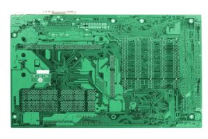
A copper design may look acceptable in CAD software but still violate the manufacturing capability of the selected PCB supplier.
For this reason, designers should confirm minimum trace/space, drill sizes, copper thickness, board thickness, layer count, and other fabrication parameters before production.
Conclusion
PCB Copper Pouring is much more than simply filling unused PCB space with copper. Properly designed copper areas can improve grounding, reduce impedance, increase current capacity, support thermal management, and improve EMI performance.
At the same time, poor copper distribution or inappropriate grounding can create signal-integrity, soldering, thermal, and manufacturing problems.
A reliable copper-pour strategy should therefore consider the entire PCB lifecycle—from schematic and layout to fabrication, assembly, inspection, and final testing.
For engineers developing prototypes or production electronics, working with an integrated manufacturing partner can simplify this process. GOPCBA provides PCB fabrication, component sourcing, SMT/THT assembly, testing, and related manufacturing services to support projects from prototype development through production. Contact GOPCBA for a PCB Project