Multilayer PCB Lamination Stackup
A reliable Multilayer PCB Stackup is essential for controlling signal integrity, impedance, power distribution, and overall PCB manufacturing quality. As PCB layer counts and signal speeds continue to increase, engineers need to carefully consider the relationship between copper thickness, dielectric thickness, material properties, trace width, trace spacing, and layer configuration.
The same discipline applies to Multilayer PCB Stackup, where a small process drift turns into a large yield loss.
A properly designed PCB Lamination structure can support complex product requirements while providing predictable electrical performance and stable manufacturing results.
For projects requiring advanced fabrication capabilities, engineers can also review PCB Manufacturing Services to understand available PCB structures, materials, copper weights, surface finishes, and manufacturing capabilities.
Why Is PCB Lamination Important?
The lamination structure determines how individual copper layers, prepreg, and core materials are combined into a finished multilayer PCB.
A suitable stackup can help engineers:
- Achieve the required finished board thickness
- Control characteristic impedance
- Maintain appropriate dielectric spacing
- Optimize power and ground distribution
- Reduce signal integrity problems
- Support high-speed and high-frequency signals
- Improve manufacturability and production consistency
- Meet mechanical and electrical design requirements
Different electronic products may require completely different stackup configurations. High-speed communication boards, industrial controllers, medical electronics, AI hardware, power electronics, and telecommunications equipment may all have different requirements.
Impedance Design Parameters for Multilayer PCBs

Reviewing Multilayer PCB Stackup before the first article is built saves rework later in the run.
Impedance Control depends on several interconnected PCB parameters. When designing a controlled-impedance board, engineers should consider the complete stackup rather than adjusting trace width alone.
1. Copper Thickness for Inner and Outer Layers
Copper thickness directly affects trace geometry and electrical characteristics.
A typical multilayer PCB may use different finished copper thicknesses for outer and inner layers. For example:
| PCB Layer | Example Finished Copper Thickness |
|---|---|
| Outer Layer | 1 oz |
| Inner Layer | 0.5 oz |
| Inner Layer | 1 oz |
The actual copper thickness should always be determined according to the selected manufacturing specification and required current-carrying capacity.
For high-current designs, heavy copper may be required. For high-density and high-speed designs, thinner copper may provide greater flexibility for fine trace-and-space requirements.
Engineers should therefore confirm the manufacturer’s actual finished copper specifications before completing the PCB layout.
For detailed manufacturing limits, designers can refer to PCB Capabilities when selecting layer counts, copper weights, board thicknesses, trace spacing, and other fabrication parameters.
2. Solder Mask Thickness
Solder mask also affects the electrical environment around surface traces and should be considered when accurate impedance calculations are required.
Typical parameters may include:
| Parameter | Example Value |
|---|---|
| Solder Mask Thickness on Substrate | 1.0 mil |
| Solder Mask Thickness Above Copper | 0.6 mil |
| Solder Mask Between Conductors | 1.0 mil |
| Approximate Solder Mask Dielectric Constant | 3.8 |
These values are examples rather than universal manufacturing specifications. Actual solder mask thickness and dielectric properties can vary depending on the selected material and manufacturing process.
Documenting Multilayer PCB Stackup keeps assembly, inspection and test teams working from the same numbers.
For precision-controlled designs, engineers should use manufacturer-provided material data instead of relying solely on generic values.
3. Understanding PCB Lamination Stackup Naming
A multilayer PCB stackup normally consists of copper layers, prepreg, and core materials.
The basic structure can be represented as:
For Multilayer PCB Stackup, the figures that matter are measured rather than assumed.
Copper Layer → Dielectric → Copper Layer → Dielectric → Core → Dielectric → Copper Layer
The exact configuration depends on the total number of PCB layers and the electrical requirements of the design.
For example, a four-layer PCB may use a structure similar to:
L1 Signal / L2 Ground / L3 Power / L4 Signal
A higher-layer-count PCB may use additional signal, ground, and power planes to improve routing density, return-current paths, and power integrity.
Every change in materials, stencils or profiles feeds back into Multilayer PCB Stackup.
When designing a stackup, engineers should consider:
- Signal layer distribution
- Ground plane placement
- Power plane placement
- Dielectric thickness
- Copper thickness
- Controlled-impedance requirements
- Via structures
- Manufacturing availability
- Finished board thickness
A good stackup should be electrically effective and manufacturable at the same time.
Using an Impedance Calculator for PCB Design
For controlled-impedance designs, engineers normally calculate the required trace width and spacing according to the target impedance and selected stackup.
The calculation should consider parameters such as:
- Target impedance
- Trace width
- Trace spacing
- Copper thickness
- Dielectric thickness
- Dielectric constant (Dk)
- Reference plane
- Signal layer configuration
- Solder mask characteristics
For example, a high-speed differential pair may require a specific differential impedance. The trace width and spacing must then be calculated based on the actual dielectric geometry between the signal layer and reference plane.
The calculation should be performed using the actual manufacturing stackup rather than an assumed generic PCB structure.
A short checklist for Multilayer PCB Stackup is usually enough to catch problems before they reach the customer.
How to Design a Controlled-Impedance PCB Stackup
Step 1: Define the Target Impedance
First determine the electrical requirements of the design.
Common requirements may include:
- Single-ended impedance
- Differential impedance
- High-speed interface requirements
- RF impedance
- Power integrity requirements
The required impedance should be defined by the circuit and interface specification before PCB layout begins.
Step 2: Select the PCB Material
The PCB material determines important electrical and mechanical properties.
Engineers should consider:
- Dielectric constant (Dk)
- Dissipation factor (Df)
- Glass transition temperature (Tg)
- Thermal performance
- Moisture resistance
- Frequency characteristics
- Manufacturing availability
Standard FR-4 materials may be sufficient for many applications, while high-speed or RF designs may require specialized high-frequency materials.
Step 3: Select the Stackup
Once the material is selected, choose a stackup that provides the required combination of:
- Layer count
- Board thickness
- Copper thickness
- Prepreg thickness
- Core thickness
- Signal/reference-plane spacing
The selected stackup should be available from the PCB manufacturer and should correspond closely to the parameters used during impedance calculation.
Step 4: Calculate Trace Width and Spacing
After the stackup is determined, calculate the required trace width and spacing for the target impedance.
Buyers who understand Multilayer PCB Stackup ask better questions during supplier audits.
For differential pairs, both trace width and pair spacing are important.
For single-ended traces, the relationship between trace width, dielectric thickness, copper thickness, and reference-plane distance must be considered.
Step 5: Verify the Design Before Manufacturing
Before releasing the PCB for production, verify:
- Layer count
- Stackup sequence
- Finished board thickness
- Copper thickness
- Trace width
- Trace spacing
- Differential-pair geometry
- Via structure
- Reference planes
- Material selection
- Impedance requirements
A DFM review can identify potential manufacturing problems before production begins.
For projects requiring engineering assistance, PCB Design and DFM Support can be considered during the pre-production stage.
Training and traceability both support Multilayer PCB Stackup on a busy production line.
Important Considerations for Multilayer PCB Lamination
PP Thickness Is Not Simply the Supplier’s Original Thickness
One important consideration in PCB Lamination is that the prepreg thickness specified in a finished stackup represents the compressed thickness after lamination rather than necessarily the original supplied thickness.
During lamination, resin flows and the prepreg is compressed according to the material system, copper pattern, pressure, temperature, and manufacturing conditions.
Therefore, engineers should use the manufacturer’s finished stackup data when performing impedance calculations.
Dk Values May Differ From Generic Material Datasheets
The dielectric constant used for PCB impedance calculations may not always correspond directly to a single nominal value published in a material datasheet.
Actual electrical behavior can be influenced by:
- Resin content
- Glass weave
- Frequency
- Material construction
- Lamination conditions
- Signal geometry
For precision Impedance Control, the manufacturer should provide appropriate stackup and material parameters for the actual production configuration.
Finished Copper Thickness Should Be Used
The copper thickness specified in a stackup should be understood in the context of finished PCB copper thickness.
Manufacturing processes such as plating, etching, surface preparation, and other treatments can affect the final copper geometry.
The same discipline applies to Multilayer PCB Stackup, where a small process drift turns into a large yield loss.
Therefore, engineers should distinguish between:
- Starting copper foil thickness
- Plated copper thickness
- Finished copper thickness
Using the wrong copper value in impedance calculations can result in inaccurate trace-width requirements.
Multilayer PCB Stackup for High-Speed Designs
High-speed PCB designs require particular attention to layer arrangement and signal return paths.
A typical high-speed architecture may place critical signal layers adjacent to solid reference planes. This helps create a more controlled electromagnetic environment and provides a shorter return-current path.
A practical stackup may include:
L1 — High-Speed Signals
L2 — Ground Plane
L3 — Power / Signals
L4 — Signals
L5 — Ground Plane
L6 — High-Speed Signals
Reviewing Multilayer PCB Stackup before the first article is built saves rework later in the run.
The actual configuration depends on the application, routing density, impedance requirements, and manufacturing constraints.
For complex applications, High-Speed PCB Manufacturing should be evaluated together with material selection, impedance requirements, layer structure, and manufacturing capability.
How Many Layers Can a Multilayer PCB Have?
Multilayer PCBs can range from relatively simple four-layer structures to highly complex boards with dozens of layers.
The required layer count depends on:
- Circuit complexity
- Component density
- Routing requirements
- Power distribution
- Signal integrity
- EMI/EMC requirements
- Mechanical dimensions
- Manufacturing cost
More layers do not automatically mean better performance. The objective is to select the minimum practical layer count that satisfies electrical, mechanical, thermal, and manufacturing requirements.
Documenting Multilayer PCB Stackup keeps assembly, inspection and test teams working from the same numbers.
For advanced projects, PCBA Manufacturing Capabilities can help engineers evaluate whether a proposed board structure is suitable for production.
PCB Lamination and Manufacturing Quality
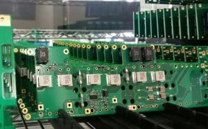
Lamination is one of the most important processes in multilayer PCB fabrication because it directly affects the physical relationship between individual layers.
Manufacturing control should address:
- Lamination temperature
- Lamination pressure
- Heating and cooling profiles
- Resin flow
- Layer alignment
- Registration accuracy
- Finished board thickness
- Internal bonding quality
Poor lamination control may result in dimensional variation, layer misregistration, delamination, or changes in electrical performance.
For Multilayer PCB Stackup, the figures that matter are measured rather than assumed.
For high-reliability electronics, the PCB manufacturer should maintain documented process controls and inspection procedures throughout fabrication and assembly.
PCB Assembly After Fabrication
After the multilayer PCB has been fabricated, it can proceed to component assembly and testing.
Depending on the product requirements, the assembly process may include:
- Solder paste printing
- SPI inspection
- SMT component placement
- Reflow soldering
- THT component insertion
- Wave or selective soldering
- AOI inspection
- X-ray inspection
- ICT or functional testing
- Final inspection
A manufacturer capable of combining PCB fabrication and assembly can simplify supply-chain management and reduce coordination between different suppliers.
For prototype and production projects, PCB Assembly Services can support SMT, THT, mixed-technology, turnkey, component sourcing, inspection, testing, and final assembly requirements.
Every change in materials, stencils or profiles feeds back into Multilayer PCB Stackup.
What Engineers Should Confirm Before Ordering a Multilayer PCB
Before production, confirm the following information with the PCB manufacturer:
Electrical Requirements
- Required single-ended impedance
- Required differential impedance
- Signal frequency
- Critical interfaces
- Controlled-impedance layers
- Differential-pair requirements
Stackup Requirements
- Number of layers
- Core materials
- Prepreg materials
- Dielectric thickness
- Copper thickness
- Finished board thickness
- Reference-plane arrangement
Manufacturing Requirements
- Minimum trace width
- Minimum spacing
- Minimum drill size
- Via structure
- Surface finish
- Solder mask
- Panelization requirements
Quality Requirements
- Material certification
- Impedance testing
- Electrical testing
- AOI
- X-ray inspection where required
- Dimensional inspection
- Final quality inspection
Clear communication between the PCB designer and manufacturer can significantly reduce manufacturing risk.
Conclusion
A properly engineered Multilayer PCB Stackup is the foundation for reliable high-density and high-speed PCB design. Copper thickness, dielectric thickness, material Dk, trace geometry, reference planes, and lamination conditions all work together to determine the final electrical performance of the board.
For controlled-impedance applications, engineers should avoid designing the stackup independently from the manufacturing process. Instead, the PCB stackup, impedance calculation, material selection, and fabrication capabilities should be evaluated as one integrated system.
By selecting a practical PCB Lamination structure, calculating trace geometry from actual manufacturing parameters, and verifying the design before production, engineers can achieve more predictable Impedance Control, better signal integrity, and improved manufacturing consistency.
A short checklist for Multilayer PCB Stackup is usually enough to catch problems before they reach the customer.
For projects from prototype development to production, GOPCBA’s PCB and PCBA Manufacturing Services provide an integrated manufacturing approach covering PCB fabrication, component sourcing, SMT/THT assembly, testing, and final product integration.