HDI PCB: Structure, Materials, Manufacturing Process, Advantages, Applications, and Design Guide
Modern electronic products are becoming smaller, faster, smarter, and more powerful. Smartphones, laptops, home appliances, medical devices, aerospace systems, automotive electronics, advanced communication equipment, and countless other electronic products have become essential to everyday life. As these products continue to evolve, manufacturers and designers face increasing pressure to integrate more functionality into smaller form factors while maintaining high electrical performance and long-term reliability.
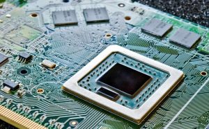
To meet these demands, PCB technology must support higher component density, finer routing, faster signal transmission, and increasingly complex interconnections. High-Density Interconnect (HDI) PCB technology provides an effective solution by enabling a large number of electronic components and interconnections to be integrated into a compact circuit board.
Through advanced via technologies, fine-pitch routing, sequential lamination, and optimized stackup structures, HDI PCBs can significantly increase wiring density while reducing board size and weight. At the same time, shorter signal paths can contribute to improved signal integrity and electrical performance.
As a result, HDI PCB technology has become an important solution for modern electronic products that require miniaturization, high performance, and reliable high-density interconnection.
What Is an HDI PCB?
An HDI PCB is a printed circuit board manufactured using advanced interconnection technologies to achieve higher wiring density and greater circuit complexity within a limited physical area.
Unlike conventional PCBs that primarily rely on through-hole vias, HDI boards commonly incorporate microvias, blind vias, buried vias, fine-pitch traces, and advanced sequential lamination technologies. These features allow designers to create more compact routing structures and accommodate high-pin-count components such as BGAs and other fine-pitch packages.
The main characteristics of HDI PCBs include:
- Higher component and routing density
- Smaller via sizes
- Finer trace widths and spacing
- Shorter electrical paths
- Better utilization of PCB layers
- Support for high-pin-count components
- Reduced board size and weight
- Improved signal integrity when properly designed
- Greater flexibility for complex circuit layouts
The combination of miniaturization and high electrical performance makes HDI technology particularly valuable in smartphones, automotive electronics, medical devices, telecommunications equipment, aerospace systems, and other advanced applications.
HDI PCB Structure and Stackup
The structure of an HDI PCB depends heavily on its interconnection architecture. Unlike conventional multilayer boards, HDI PCBs use different types of vias and sequentially laminated layers to maximize available routing space.
HDI PCB Via Structure
The key interconnection technologies used in HDI boards include blind vias, buried vias, microvias, and via-in-pad structures.
Blind Vias
A blind via connects an outer layer of the PCB to one or more internal layers without passing through the entire board.
Because blind vias occupy less vertical space than traditional through-hole vias, they allow designers to use internal routing areas more efficiently. They are especially useful for connecting surface-mounted components to selected internal signal layers.
Buried Vias
A buried via connects two or more internal PCB layers but does not extend to the outer surface of the board.
Since buried vias are contained entirely within the PCB structure, they can provide additional internal interconnection capacity without consuming valuable surface routing space. This makes them useful for high-density multilayer designs.
Microvias
Microvias are very small vias, typically formed using laser drilling rather than conventional mechanical drilling. They are used to connect adjacent layers or selected layers within an HDI structure.
Microvias can be arranged as stacked or staggered structures depending on the design and manufacturing process. Their small size allows designers to route signals between dense component pads and internal layers while maintaining compact PCB dimensions.
Microvia technology is one of the fundamental elements of HDI manufacturing because it supports fine-pitch component placement and high-density routing.
Via-in-Pad
Via-in-pad places a microvia directly within a component pad, commonly underneath fine-pitch packages such as BGAs.
This configuration eliminates the need for a conventional trace extending from the pad to a nearby via. As a result, valuable PCB surface area can be saved and component escape routing can be improved.
However, via-in-pad structures require appropriate manufacturing controls, including proper filling and planarization where necessary, to prevent soldering defects such as solder wicking.
HDI PCB Stackup
An HDI stackup consists of multiple copper and dielectric layers arranged to provide sufficient routing capacity, controlled impedance, power distribution, and signal integrity.
Unlike a conventional multilayer PCB, an HDI structure often uses sequential lamination to add dielectric and copper layers around a core. This manufacturing approach enables designers to introduce additional microvia layers where routing density is highest.
Common HDI stackup configurations include 1+N+1, 2+N+2, and 3+N+3 structures.
1+N+1 HDI Stackup
The 1+N+1 structure is one of the most common basic HDI configurations.
In this structure, one HDI buildup layer is added to each side of the central core. Microvias provide interconnections between the outer buildup layers and the underlying layers.
The relatively simple structure provides a good balance between routing density, manufacturing complexity, and cost. It is commonly considered for consumer electronics, communication products, and moderately complex electronic devices.
2+N+2 HDI Stackup
The 2+N+2 structure contains two buildup layers on both sides of the central core.
Compared with 1+N+1, this architecture provides additional routing layers and greater flexibility for complex component escape routing. It can accommodate higher-density components and more complicated electrical connections.
This configuration is suitable for applications such as advanced computing systems, networking equipment, automotive electronics, and other products that require greater routing capacity and electrical performance.
3+N+3 HDI Stackup
The 3+N+3 configuration uses three buildup layers on each side of the core.
This advanced architecture provides substantially greater routing density and is suitable for highly compact and electrically complex designs. Multiple microvia layers can be used to support dense component interconnections and high-speed signal routing.
Applications may include advanced computing platforms, sophisticated medical electronics, aerospace systems, and other high-performance products where space, routing density, and electrical requirements are particularly demanding.
The appropriate stackup should always be selected according to component density, signal-speed requirements, layer count, impedance requirements, thermal constraints, manufacturing capabilities, and cost targets.
Materials Used in HDI PCBs
Material selection plays a critical role in HDI PCB manufacturing because these boards must support fine circuitry, dense interconnections, high-speed signals, thermal loads, and demanding reliability requirements.
The major materials used in HDI PCBs include laminates, copper foil, prepreg, solder mask, and surface-finish materials.
FR-4 Laminate
FR-4 remains one of the most widely used base materials for HDI PCBs because it provides a practical balance between electrical performance, mechanical strength, manufacturability, and cost.
Standard FR-4 materials are suitable for many general-purpose applications. For higher-speed applications, designers may select enhanced FR-4 materials with more controlled dielectric properties and lower signal losses.
Material selection should consider dielectric constant, dissipation factor, thermal performance, glass-transition temperature, coefficient of thermal expansion, and compatibility with the intended lamination process.
Copper Foil
Copper foil forms the conductive layers of an HDI PCB.
Thin copper foil is often preferred for fine-line HDI structures because it allows manufacturers to produce smaller trace widths and spacing while maintaining better process control.
The appropriate copper thickness depends on current requirements, signal characteristics, thermal considerations, manufacturing capability, and mechanical reliability requirements.
Copper Thickness
Copper thickness directly affects current-carrying capability, electrical resistance, thermal performance, and manufacturing characteristics.
Thinner copper can facilitate fine-line routing and microvia fabrication, while thicker copper may be required for power circuits and high-current applications.
Therefore, copper thickness should be carefully optimized rather than selected solely according to conventional PCB requirements.
Prepreg
Prepreg is a resin-based dielectric material used between PCB layers. During lamination, the resin flows and cures to bond the layers together while providing electrical insulation.
For HDI structures, prepreg selection is especially important because resin flow, dielectric thickness, thermal expansion, and lamination characteristics can affect microvia reliability, impedance control, and layer alignment.
A properly selected prepreg system helps maintain mechanical integrity and dimensional stability throughout manufacturing and operation.
Solder Mask
Solder mask protects exposed copper areas and helps prevent solder bridges during PCB assembly. In HDI designs, solder mask registration and opening accuracy become particularly important because of fine-pitch components and small pads.
Surface Finish
The surface finish protects exposed copper from oxidation and provides a suitable surface for component soldering.
Common surface finishes include:
- ENIG (Electroless Nickel Immersion Gold): Suitable for fine-pitch components and applications requiring good surface flatness and reliability.
- Immersion Silver: Provides a relatively flat surface and good solderability and can be suitable for certain high-density applications.
- OSP (Organic Solderability Preservative): A cost-effective surface finish suitable for many high-volume applications.
- ENEPIG: Can be considered for demanding applications requiring excellent surface characteristics and compatibility with advanced assembly technologies.
The appropriate surface finish depends on component package requirements, soldering processes, storage conditions, reliability targets, and overall project cost.
HDI PCB Manufacturing Process
Compared with conventional multilayer PCB manufacturing, HDI PCB fabrication requires tighter dimensional control and more sophisticated processing.
Small variations in drilling, imaging, plating, lamination, or registration can affect the reliability of microvias and fine-line circuitry. Therefore, HDI manufacturing requires advanced equipment, process control, inspection systems, and experienced engineering personnel.
Step 1: Laser Drilling and Microvia Formation
Laser drilling is one of the most important processes in HDI PCB manufacturing.
Unlike conventional mechanical drilling used for larger through-holes, laser drilling creates extremely small and accurately positioned microvias. Depending on the material system and process requirements, UV or CO₂ laser systems may be used.
The quality of laser drilling directly affects microvia diameter, wall condition, alignment, and subsequent copper plating reliability.
Step 2: Through-Hole Drilling and Copper Plating
Where through-holes are required, mechanical drilling is typically performed before or during the appropriate fabrication stage.
The drilled holes are then metallized through chemical and electrolytic copper processes. Copper plating creates an electrically conductive path between PCB layers and establishes the required copper thickness.
For HDI products, plating quality is particularly important because microvias and other small interconnections must withstand thermal and mechanical stresses throughout the product’s operating life.
Step 3: Sequential Lamination
Sequential lamination is a defining feature of many HDI manufacturing processes.
Additional dielectric and copper layers are built onto the core through repeated lamination cycles. Microvias are then formed to connect the newly added layers to the appropriate conductive structures.
Advanced HDI boards may require several sequential lamination cycles depending on the stackup and interconnection architecture.
Step 4: Circuit Imaging and Etching
Fine-line circuit patterns are transferred onto the copper layers using high-precision imaging processes.
After imaging, unwanted copper is removed through controlled etching to form the required circuit pattern.
Because HDI designs frequently use fine traces and tight spacing, imaging and etching processes require excellent registration and dimensional control.
Step 5: Surface Finish
After the external circuitry has been completed and inspected, an appropriate surface finish is applied.
The surface finish protects exposed copper from oxidation and provides suitable solderability for PCB assembly.
Step 6: Electrical Testing and Inspection
HDI PCBs require comprehensive inspection and electrical testing.
Depending on the product, testing may include:
- Automated optical inspection (AOI)
- Electrical continuity and isolation testing
- Microsection analysis
- X-ray inspection
- Impedance testing
- Dimensional inspection
- Microvia reliability evaluation
The exact testing strategy depends on the board structure, application requirements, component technology, and reliability standards.
Advantages of HDI PCBs
The major advantage of HDI PCB technology is its ability to combine compact dimensions with high routing density and advanced electrical performance.
Higher Component Density
Microvias, fine traces, small pads, and optimized layer structures allow more components and interconnections to be integrated into a limited area.
This enables designers to create more sophisticated products without proportionally increasing PCB dimensions.
Product Miniaturization
Miniaturization is one of the primary reasons manufacturers adopt HDI technology.
Smaller vias and finer routing structures allow the PCB to occupy less space. This is especially valuable in smartphones, wearable electronics, portable medical devices, automotive electronics, and other space-constrained products.
Improved Signal Integrity
HDI designs can reduce signal-path length and provide more controlled routing structures.
Shorter interconnections can help reduce parasitic capacitance and inductance, while an appropriately engineered stackup can support controlled impedance and reduce signal-integrity problems.
However, HDI technology alone does not automatically guarantee good signal integrity. Proper stackup design, grounding, return-path management, impedance control, and routing practices remain essential.
Improved Routing Efficiency
Microvias and sequential buildup layers provide additional routing opportunities.
Instead of routing every connection through large through-hole structures, designers can use localized microvia connections to improve component escape routing and layer utilization.
This is particularly beneficial for fine-pitch BGA and other high-pin-count packages.
Reduced PCB Weight
HDI technology can help reduce PCB size and, in some designs, reduce the amount of material required.
Lower board weight can be particularly valuable in portable electronics, aerospace systems, drones, and other weight-sensitive applications.
Enhanced Reliability
When properly designed and manufactured, HDI PCBs can provide highly reliable interconnections.
Modern HDI manufacturing processes allow microvia structures, layer registration, plating, and lamination to be tightly controlled. Nevertheless, reliability depends on material selection, via design, aspect ratio, thermal cycling, manufacturing quality, and application conditions.
HDI PCB Applications
HDI technology is widely used wherever electronic systems require high functionality within a limited physical footprint.
Smartphones and Consumer Electronics
Smartphones are among the most recognizable applications of HDI PCBs.
A modern smartphone must integrate processors, memory, cameras, sensors, wireless communication circuits, power-management components, and other functions into an extremely limited space.
HDI technology enables these components to be interconnected using compact, high-density routing structures.
Other consumer electronics applications include tablets, smartwatches, wearable devices, cameras, gaming equipment, and portable electronic products.
Automotive Electronics
HDI PCBs are increasingly used in automotive electronics, including electric vehicles, advanced driver-assistance systems (ADAS), infotainment systems, camera modules, radar-related electronics, and vehicle control systems.
These applications require compact circuit designs, reliable signal transmission, thermal stability, and long-term mechanical reliability.
Medical Devices
Medical electronics often require small dimensions without sacrificing electrical performance or reliability.
HDI PCBs can be used in portable monitoring devices, diagnostic equipment, imaging systems, wearable medical electronics, and other compact medical products.
Telecommunications Equipment
Telecommunication systems require high-speed data transmission and efficient signal routing.
HDI PCBs can be used in routers, wireless communication equipment, networking hardware, base-station electronics, and other high-speed communication systems.
Aerospace and Defense
Aerospace and defense electronics place strong emphasis on weight, reliability, environmental resistance, and electrical performance.
HDI technology can help reduce system size and weight while providing dense interconnection structures for navigation equipment, radar electronics, satellite systems, avionics, and other advanced electronic platforms.
Industrial Automation
Industrial automation equipment, robotics, machine-vision systems, controllers, and smart manufacturing platforms often require multiple electronic functions to be integrated into compact assemblies.
HDI PCBs can help improve integration density while supporting high-speed data processing and reliable electrical interconnection.
HDI PCB Design Guidelines
Successful HDI PCB design requires careful planning from the beginning of the project.
The designer must consider component selection, stackup, microvia structures, impedance, signal integrity, thermal management, manufacturability, reliability, and cost.
Select the PCB Manufacturer Early
Choosing an experienced HDI PCB manufacturer during the early design stage can significantly reduce manufacturing risks.
Not every PCB manufacturer has the equipment or process capability required for advanced microvias, fine-line circuits, sequential lamination, via-in-pad, and complex HDI stackups.
Early communication with the manufacturer allows designers to align the design with actual manufacturing capabilities.
Optimize Microvia Usage
Microvias provide excellent routing flexibility, but excessive use can increase manufacturing complexity and cost.
Designers should use microvias strategically and select appropriate via diameters, capture pads, aspect ratios, stacking structures, and staggered configurations.
The objective should be to achieve the required routing density without unnecessarily increasing fabrication difficulty.
Maintain Signal Integrity
Signal integrity becomes increasingly important as data rates increase.
HDI PCB designers should carefully manage:
- Controlled impedance
- Trace width and spacing
- Reference planes
- Return-current paths
- Differential-pair routing
- Via transitions
- Crosstalk
- Power distribution
- Grounding structures
A well-designed HDI stackup can provide better control of high-speed signal paths and reduce unwanted parasitic effects.
Address Thermal Management
High component density can increase localized heat generation.
Thermal management should therefore be considered during the initial PCB design stage rather than after the layout has been completed.
Depending on the application, thermal vias, copper planes, heat spreaders, appropriate component placement, and suitable PCB materials may be used to improve heat dissipation.
Apply Design for Manufacturability (DFM)
Design for Manufacturability (DFM) is essential for HDI PCB projects.
A design that looks excellent electrically may still be difficult or expensive to manufacture if it exceeds the manufacturer’s process capabilities.
DFM considerations should include:
- Minimum trace width and spacing
- Microvia diameter
- Via aspect ratio
- Pad dimensions
- Layer-to-layer registration
- Copper thickness
- Lamination requirements
- Surface-finish compatibility
- Panel utilization
- Inspection and testing requirements
Working with the manufacturer during the design stage can help reduce redesigns, improve yield, and control production costs.
HDI PCB vs. Standard PCB
The difference between an HDI PCB and a conventional PCB is not simply the physical size or number of layers.
Standard PCBs remain highly effective for many general-purpose applications. However, when circuit density, component pitch, signal speed, or space constraints become more demanding, HDI technology can provide significant advantages.
| Feature | Standard PCB | HDI PCB |
|---|---|---|
| Via Technology | Primarily through-hole vias | Microvias, blind vias, buried vias, and via-in-pad |
| Routing Density | Low to medium | Very high |
| Board Size | Larger for complex circuits | More compact |
| Signal Performance | Suitable for many conventional applications | Well suited to high-speed and high-density designs |
| Stackup | Conventional multilayer stackup | Often uses sequential buildup and HDI structures |
| Component Density | Low to medium | High to very high |
| Manufacturing Complexity | Relatively low | High |
| Cost | Generally lower | Generally higher |
| Typical Applications | General electronics, power systems, control boards | Smartphones, medical devices, automotive electronics, aerospace, telecommunications |
The comparison demonstrates that standard PCBs remain cost-effective for straightforward designs, while HDI PCBs become increasingly valuable when miniaturization, routing density, high-speed performance, and advanced component packaging are critical.
How to Choose an HDI PCB Manufacturer
Selecting an HDI PCB manufacturer should involve more than comparing unit prices.
Because HDI fabrication requires advanced equipment and tight process control, manufacturers should be evaluated based on engineering capability, production capacity, quality systems, testing capabilities, and experience with similar products.
Engineering Support
A capable HDI PCB manufacturer should provide engineering support throughout the development process.
This may include recommendations for:
- Stackup configuration
- Microvia structures
- Material selection
- Controlled impedance
- Trace and spacing rules
- Via-in-pad implementation
- Thermal management
- DFM optimization
Early engineering collaboration can prevent costly design revisions later in the project.
Quality Control
Quality control is particularly important because HDI manufacturing involves fine lines, microvias, sequential lamination, and precise layer registration.
A reliable manufacturer should maintain a comprehensive quality-management system and use appropriate inspection and testing procedures.
Relevant certifications and compliance should also be evaluated according to the requirements of the target market and application.
Prototype Capability
Rapid and reliable prototyping is essential for validating HDI designs before mass production.
A qualified manufacturer should be capable of producing prototypes that accurately reflect the intended production process. Prototype validation can identify problems related to stackup, signal integrity, component assembly, microvias, and thermal performance before large-scale manufacturing begins.
Production Capacity
After prototype validation, the project may transition to volume production.
The manufacturer should have sufficient production capacity and process stability to maintain consistent quality and yield across different production volumes.
Important factors include equipment capability, production scheduling, process control, material management, and scalability.
Testing Capabilities
Because HDI PCBs contain highly dense interconnections, comprehensive testing is essential.
Depending on project requirements, testing may include electrical testing, impedance testing, AOI, X-ray inspection, microsection analysis, dimensional inspection, and reliability testing.
A manufacturer’s ability to identify and control potential microvia and internal-layer defects is an important indicator of its HDI manufacturing capability.
Why Choose Kingda for HDI PCB Manufacturing?
For advanced electronics, selecting the right HDI PCB manufacturer can have a direct impact on product reliability, development efficiency, manufacturing yield, and overall cost.
Kingda can support HDI PCB projects that require high-density routing, fine-line structures, microvia technology, complex multilayer construction, and demanding electrical performance.
An experienced HDI manufacturing partner should be able to support customers from initial engineering analysis and stackup development through prototype production, testing, and volume manufacturing.
For projects involving compact electronics, high-speed signals, fine-pitch components, or complex interconnections, working closely with Kingda during the early design stage can help optimize the PCB architecture for both performance and manufacturability.
Conclusion
High-Density Interconnect (HDI PCB) technology has become an important part of modern electronic product development.
As electronic devices continue to become smaller, faster, lighter, and more functional, conventional PCB structures may not always provide sufficient routing density or packaging flexibility. HDI technology addresses these challenges through microvias, blind vias, buried vias, fine-line routing, via-in-pad structures, and sequential lamination.
From smartphones and automotive electronics to medical equipment, telecommunications, aerospace, defense, and industrial automation, HDI PCBs enable designers to integrate more functionality into increasingly compact products.
However, successful HDI PCB development requires more than simply reducing via sizes or increasing routing density. Material selection, stackup design, signal integrity, thermal management, DFM, manufacturing capability, testing, and reliability must all be considered as part of an integrated engineering process.
By working with an experienced HDI PCB manufacturer such as Kingda from the early design stage, product developers can better balance miniaturization, electrical performance, manufacturability, reliability, and cost. As electronic systems continue to evolve toward higher density and greater functionality, HDI PCB technology will remain a key enabler of next-generation electronics.