PCB Copper Pour Design Guide: Importance, Benefits, and Key Design Considerations
Copper pouring is one of the most important techniques in modern Printed Circuit Board Design. By filling unused areas of a PCB layer with copper, engineers can improve grounding performance, reduce electromagnetic interference, enhance current carrying capability, and optimize overall circuit stability.
However, copper pour is not simply a process of filling empty space with copper. Incorrect copper placement or poor grounding strategies may create unexpected problems, including signal interference, unstable circuits, and manufacturing difficulties.
For this reason, professional PCB Copper Pour Design requires careful planning based on electrical performance, signal frequency, manufacturing capability, and application requirements.
What Is PCB Copper Pour?
Definition of Copper Pour in PCB Design
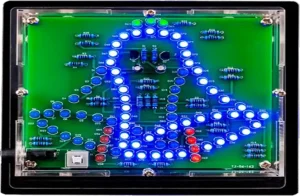
A copper pour refers to the process of adding large copper areas to unused regions of a PCB layer.
These copper areas are usually connected to:
- Ground networks
- Power networks
- Shielding structures
Copper pours are commonly used in multilayer circuit boards to create stable reference planes and improve electrical performance.
The main purposes include:
- Reducing ground impedance
- Improving current distribution
- Reducing voltage drop
- Enhancing electromagnetic shielding
- Improving heat dissipation
A properly designed copper layer becomes an important part of the electrical system rather than just an empty copper area.
Why Is PCB Copper Pour Important?
1. Improving Grounding Performance
One of the primary purposes of copper pouring is improving the grounding structure.
A large copper area connected to ground can:
- Reduce ground resistance
- Provide shorter return paths
- Minimize ground noise
- Improve circuit stability
For high-speed circuits, a solid ground reference is especially important because signal return currents need a low-impedance path.
Professional PCB Ground Plane Design helps control signal return paths and improves overall signal integrity.
For advanced circuit solutions, engineers can utilize professional PCB Design Services to optimize grounding and layer structures before manufacturing.
2. Reducing Electromagnetic Interference (EMI)
High-frequency signals can generate electromagnetic radiation if return currents are not properly controlled.
A well-designed copper pour can reduce:
- Signal loop area
- Noise radiation
- Crosstalk between circuits
- Electromagnetic interference
However, copper must be properly connected to ground.
A poorly grounded copper area may become an antenna that increases noise instead of reducing it.
3. Improving Heat Dissipation
Copper has excellent thermal conductivity.
Copper pours can help transfer heat away from:
- Power components
- Voltage regulators
- High-current circuits
- Heat-generating devices
By improving thermal performance, copper areas can extend component lifespan and increase product reliability.
Types of PCB Copper Pour Structures
Solid Copper Pour
A solid copper area completely fills the available space on the PCB layer.
Advantages:
- Excellent current carrying capability
- Strong grounding performance
- Better EMI shielding
However, solid copper may create manufacturing challenges during soldering.
Potential problems include:
- PCB warping
- Copper imbalance
- Thermal stress during soldering
For this reason, manufacturers often add thermal relief structures or copper balancing techniques.
Grid Copper Pour
A grid copper pattern uses crossed copper lines instead of a completely solid area.
Advantages include:
- Reduced thermal stress
- Better manufacturing stability
- Improved heat distribution
Grid copper is often used in specific applications where mechanical stability is more important than maximum current capacity.
The correct choice depends on:
- Signal frequency
- Current requirements
- Manufacturing process
- Application environment
PCB Copper Pour Design Considerations
1. Separate Different Ground Networks
Many electronic systems contain multiple ground types, such as:
- Digital ground (DGND)
- Analog ground (AGND)
- Signal ground (SGND)
Incorrectly connecting these grounds may introduce noise into sensitive circuits.
Engineers should carefully define:
- Ground separation areas
- Connection points
- Return current paths
Different ground regions should only connect at appropriate locations according to circuit requirements.
2. Avoid Copper Islands and Floating Areas
Unused copper areas that are not connected to any electrical network are called copper islands.
Floating copper can:
- Collect electrical noise
- Create unexpected capacitance
- Affect signal performance
Engineers should remove unnecessary copper islands or connect them properly through vias and grounding structures.
3. Maintain Proper Clearance Around High-Frequency Components
High-frequency components require special attention during copper design.
For example, crystal oscillators and RF circuits are sensitive to surrounding copper structures.
Incorrect copper placement may affect:
- Frequency stability
- Signal quality
- Noise performance
Proper layout planning during PCB Layout Optimization helps prevent these issues.
Learn more about professional High-Speed PCB Design Solutions for advanced electronic applications.
4. Use Thermal Vias for Heat Transfer
Thermal vias connect copper layers to improve heat dissipation.
They are commonly used under:
- Power ICs
- LED drivers
- MOSFET components
- Voltage regulators
Benefits include:
- Lower operating temperature
- Improved reliability
- Better thermal management
5. Avoid Sharp Copper Corners
Sharp copper corners can create electromagnetic radiation problems.
From an electromagnetic perspective, sharp angles may behave like antennas and increase unwanted radiation.
Recommended practices:
- Use curved corners
- Avoid unnecessary sharp edges
- Maintain smooth copper shapes
These improvements contribute to better EMI performance.
Copper Pour in Multilayer PCB Design
Importance of Internal Copper Layers
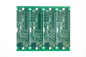
In multilayer boards, internal copper layers are often used as:
- Ground planes
- Power planes
- Signal reference layers
Proper layer planning improves:
- Signal integrity
- Power stability
- Noise reduction
A professional PCB Manufacturing Process requires accurate control of layer alignment, copper thickness, and dielectric spacing.
For complex multilayer applications, explore our Multilayer PCB Manufacturing capabilities.
Common PCB Copper Pour Mistakes
Incorrect Ground Connection
A copper area without a proper ground connection may increase noise instead of reducing it.
Always verify:
- Net connection
- Ground vias
- Reference planes
Excessive Copper Without Manufacturing Consideration
Large copper areas may cause:
- Uneven copper distribution
- Warping
- Soldering issues
Manufacturing capability should always be considered during PCB design.
Poor Return Path Planning
High-speed signals require controlled return paths.
Incorrect copper design may cause:
- Signal reflection
- Increased EMI
- Data transmission errors
How Professional PCB Manufacturers Optimize Copper Design
Experienced manufacturers follow a complete process to ensure copper structures meet electrical and production requirements.
Engineering Review
Engineers analyze:
- PCB layer stack-up
- Ground requirements
- Signal frequency
- Current capacity
Design Verification
Verification includes:
- Design rule checking
- Copper balance analysis
- Signal integrity evaluation
Manufacturing Control
During production, manufacturers control:
- Copper thickness
- Etching accuracy
- Layer alignment
- Surface quality
Assembly Testing
Final testing ensures the finished board meets electrical and mechanical requirements.
For complete production support, professional PCB Assembly Services provide integrated manufacturing solutions.
Conclusion
PCB copper pouring is a critical part of modern circuit board design. When properly implemented, copper areas improve grounding, reduce electromagnetic interference, enhance thermal performance, and increase circuit reliability.
However, copper pour design requires careful consideration of grounding methods, signal frequency, manufacturing limitations, and thermal requirements.
By combining advanced design methods with professional manufacturing capabilities, engineers can achieve stable and high-performance electronic products.
Reliable PCB Design Services and advanced production technology ensure that copper structures are optimized from prototype development to mass production.