24 PCB Design Tips to Reduce Noise and Electromagnetic Interference
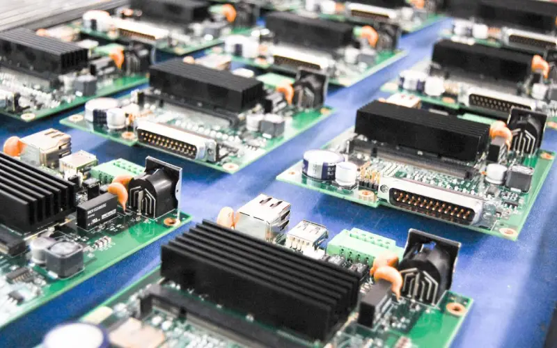
In modern electronic products, electromagnetic interference (EMI) and electrical noise are major challenges affecting system stability and performance. A well-designed PCB Circuit Board must control unwanted signals, minimize interference sources, and maintain reliable communication between electronic components.
During the PCB Design process, engineers need to consider signal routing, power distribution, grounding methods, component placement, and high-frequency behavior.
Proper design techniques not only improve product performance but also simplify the manufacturing process and improve production reliability.
gopcba provides professional PCB Design Services to help engineers develop high-performance and reliable circuit solutions:
24 Effective PCB Design Methods for Noise and EMI Reduction
1. Select the Appropriate Operating Frequency
Avoid using high-speed components when lower-speed alternatives can meet system requirements.
High-frequency devices generate more electromagnetic radiation and switching noise. Selecting the lowest suitable operating frequency can significantly reduce interference problems.
High-speed components should only be used in critical circuit areas where performance requirements demand them.
2. Use Series Resistors to Reduce Signal Oscillation
Adding series resistors to signal lines can reduce excessive rising and falling edges.
This method helps:
- Reduce signal overshoot
- Minimize ringing
- Improve signal stability
- Reduce electromagnetic radiation
Series termination is commonly used for high-speed digital signals.
3. Add Proper Damping for Relay Circuits
Relay switching can generate voltage spikes and electromagnetic noise.
Recommended solutions include:
- Flyback diodes
- RC damping circuits
- Snubber circuits
These methods protect sensitive components and improve system reliability.
4. Use the Lowest Required Clock Frequency
Clock signals are one of the strongest noise sources in electronic systems.
Using an unnecessarily high clock frequency increases:
- EMI radiation
- Signal interference
- Power consumption
Selecting the correct clock frequency helps maintain stable operation.
5. Keep Clock Generators Close to Clock Devices
Clock traces should be as short as possible.
Recommended practices:
- Place crystal oscillators near related ICs
- Minimize clock routing length
- Connect oscillator shields properly to ground
This reduces noise radiation and improves clock stability.
6. Surround Clock Areas with Ground Protection
Sensitive clock circuits should have proper grounding protection.
A ground ring or ground copper area around the clock section can reduce external interference and prevent noise coupling.
7. Place I/O Circuits Near the PCB Edge
I/O driver circuits should be placed close to the edge of the board.
Benefits include:
- Shorter signal paths
- Reduced radiation area
- Lower interference
Signals entering noisy areas should also include proper filtering and termination methods.
8. Never Leave IC Pins Floating
Unused IC pins should not remain unconnected.
They should be configured as:
- Connected to high level
- Connected to ground
- Defined as output pins
Floating pins may collect noise and create unstable circuit behavior.
9. Properly Handle Unused Operational Amplifiers
Unused operational amplifiers should be correctly configured.
Common solutions include:
- Connecting the positive input to ground
- Connecting the negative input to the output
This prevents unwanted oscillation.
10. Use 45-Degree Routing Instead of Sharp 90-Degree Corners
High-frequency signals should avoid sharp routing angles.
Using 45-degree traces helps:
- Reduce impedance changes
- Improve signal integrity
- Reduce EMI radiation
Professional PCB Design follows strict routing rules for high-speed circuits.
11. Separate Noisy and Sensitive Circuit Areas
PCB layouts should be divided according to signal characteristics.
High-noise components should be separated from sensitive circuits, including:
- Analog circuits
- RF circuits
- Sensor interfaces
- Reference voltage circuits
Proper zoning reduces unwanted signal coupling.
12. Use Proper Power and Ground Design
Power and ground networks are critical for reducing noise.
Recommended practices:
- Use wider power traces
- Minimize ground impedance
- Use dedicated ground planes
For multilayer boards, separate power and ground layers help improve electrical performance.
Learn more about our Multilayer PCB Solutions:
13. Keep Clock Signals Away from I/O Lines
Clock signals should not run parallel with:
- Communication lines
- Connectors
- External cables
Keeping distance between these signals reduces electromagnetic coupling.
14. Separate Analog and Digital Signal Routing
Analog reference signals are sensitive to digital noise.
Avoid routing:
- Analog inputs
- Reference voltage lines
near:
- Clock signals
- High-speed digital traces
This improves measurement accuracy and system stability.
15. Properly Separate Mixed-Signal Circuits
For devices containing both analog and digital sections, the layout should be carefully planned.
Recommended practices:
- Separate functional areas
- Control return current paths
- Avoid unnecessary signal crossing
16. Keep Component Pins as Short as Possible
Long component leads increase parasitic effects.
Short connections help:
- Reduce inductance
- Improve high-frequency performance
- Reduce noise generation
Decoupling capacitor placement is especially important.
17. Use Short and Thick Critical Signal Traces
Important signals should have:
- Short routing distance
- Appropriate trace width
- Good grounding reference
High-speed signals should avoid unnecessary bends and vias.
18. Protect Sensitive Signal Lines
Noise-sensitive traces should be protected from:
- High-current paths
- Switching power circuits
- High-frequency signals
Ground shielding can be used when necessary.
19. Avoid Parallel Routing Between Noise Sources and Sensitive Signals
High-current switching lines can generate strong electromagnetic fields.
Avoid routing sensitive signals parallel to these noise sources.
20. Keep Sensitive Components Away from Crystal Oscillators
Crystal oscillators produce high-frequency signals.
Sensitive circuits should maintain proper distance from oscillator areas to prevent interference.
21. Avoid Creating Large Current Loops
Large current loops increase electromagnetic radiation.
During PCB Design, engineers should minimize loop areas by controlling:
- Signal paths
- Return paths
- Ground connections
22. Reduce Signal Loop Areas
If a signal loop cannot be avoided, keep the loop area as small as possible.
Smaller loops provide:
- Lower EMI radiation
- Better signal integrity
- Improved reliability
23. Add Proper Decoupling Capacitors
Each integrated circuit should have appropriate decoupling capacitors.
Recommended design:
- One small high-frequency bypass capacitor near each IC power pin
- Additional bulk capacitors for power stability
This reduces power supply noise.
24. Select Suitable Energy Storage Capacitors
For power filtering applications, designers may consider:
- Tantalum capacitors
- Polymer capacitors
- High-performance ceramic capacitors
These components provide better charging and discharging performance compared with traditional solutions in many applications.
Factors Affecting Flexible PCB Bending Performance
Flexible PCB (FPC) products require special attention to mechanical reliability.
The bending performance of an FPC depends on both material selection and manufacturing processes.
Material Factors Affecting FPC Flexibility
Copper Foil Type
The copper foil structure has a significant impact on bending performance.
Rolled annealed copper (RA copper) generally provides better flexibility than electro-deposited copper.
Copper Thickness
For the same material type, thinner copper foil provides improved bending performance.
Adhesive Material
The substrate adhesive affects flexibility.
Materials with better flexibility characteristics are preferred for applications requiring repeated bending.
Adhesive Thickness
A thinner adhesive layer generally improves flexibility and reduces stress during bending.
Insulation Material Thickness
The thickness of the PI insulation layer directly affects flexibility.
Thinner PI materials typically provide better bending performance.
Manufacturing Factors Affecting FPC Reliability
Symmetrical Layer Structure
A balanced FPC structure improves bending reliability.
When copper layers and insulation materials have symmetrical thickness, mechanical stress is distributed more evenly during bending.
Lamination Process Control
During FPC lamination, adhesive materials must completely fill the circuit area.
Poor lamination may cause:
- Layer separation
- Reduced bending cycles
- Mechanical failure
Strict process control is essential during PCB Manufacturing.
Explore our complete PCB Manufacturing Services:
PCB Assembly Considerations for Noise Control
Noise reduction does not end after PCB fabrication.
During PCB Assembly, manufacturers must ensure:
- Correct component placement
- Proper soldering quality
- Accurate component orientation
- Reliable electrical connections
A complete manufacturing process improves product performance and long-term reliability.
Learn more about our PCB Assembly Services:
Applications Requiring Advanced EMI Control
Communication Equipment
High-speed communication products require excellent signal integrity and EMI management.
Automotive Electronics
Vehicle systems require stable operation in complex electromagnetic environments.
Medical Devices
Medical electronics require low-noise and highly reliable circuit performance.
Industrial Control Systems
Industrial equipment depends on durable PCB solutions with strong interference resistance.
Explore our PCB Applications:
Conclusion
Reducing noise and electromagnetic interference is one of the most important goals in modern PCB Design.
By applying proper grounding methods, controlling signal routing, optimizing component placement, and selecting suitable materials, engineers can significantly improve the reliability of electronic products.
From design optimization to final PCB Assembly, every manufacturing stage affects the final performance of the product.
gopcba provides professional PCB solutions, including design support, manufacturing, and assembly services for global electronics companies.
Visit: