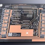
In PCB design software, the concept of “layers” is similar to the layers used in graphic design or document-editing software. However, PCB Layers are not simply virtual elements used to organize graphics, text, or colors. They correspond to the actual physical structure and manufacturing data of a printed circuit board.
As electronic products continue to become smaller and more highly integrated, PCB layouts are becoming increasingly dense. Requirements related to signal integrity, electromagnetic interference, power distribution, and routing have also become more demanding. Modern PCBs may therefore contain multiple copper layers rather than routing only on the top and bottom surfaces.
For example, many computer motherboards and other complex electronic products use four-layer, six-layer, eight-layer, or even higher-layer PCBs. Different layers can be assigned to signal routing, power distribution, and ground planes. Understanding the purpose of each layer is therefore essential for effective PCB Design.
PCB Layers and Layer Settings
In a multilayer PCB, different layers perform different functions. Signal layers are generally used for routing electrical connections, while dedicated power and ground layers can provide stable power distribution and help reduce electromagnetic interference.
Large copper areas are often used on power and ground layers to reduce impedance and improve current distribution. When a signal needs to pass between different layers, a Via is normally used to establish the electrical connection.
Designers should carefully configure the required layers before beginning PCB layout. Unused layers should be disabled or hidden when appropriate to reduce design errors and prevent unnecessary routing complexity.
For example, if a component footprint is created without properly assigning its pads to the appropriate layer, the pads may not appear correctly during PCB layout or manufacturing output. This demonstrates why layer settings are an important part of the overall PCB Design process.
Via
A Via is a plated hole used to establish an electrical connection between different conductive layers of a PCB.
During manufacturing, a hole is drilled through the PCB, and the inner wall is plated with copper. This conductive layer connects the copper structures assigned to different layers.
Depending on the PCB structure and design requirements, vias may be classified as through vias, blind vias, and buried vias. Advanced HDI boards may use microvias to support high-density interconnections.
When designing vias, several important principles should be considered.
1. Minimize unnecessary vias
Although vias are essential for multilayer routing, excessive use can increase manufacturing complexity and consume valuable routing space.
Designers should maintain sufficient clearance between vias, traces, pads, and other conductive structures.
In automated routing environments, appropriate design-rule settings can help ensure that the required clearance is maintained automatically.
2. Consider current-carrying capacity
The required via size depends partly on the amount of current that the via needs to carry.
For example, vias used to connect power planes and ground planes may require larger diameters or multiple vias in parallel to reduce electrical resistance and improve current-carrying capability.
For high-current applications, thermal performance and copper plating thickness should also be considered during the PCB design stage.
PCB Pads
PCB Pads are among the most important elements in PCB layout because they provide the electrical and mechanical interface between components and the circuit board.
Beginners often use standard circular pads without considering the actual requirements of the component. In professional PCB design, pad shape and size should be selected according to the component package, pin dimensions, assembly method, mechanical stress, thermal conditions, and current requirements.
Most PCB design software provides standard pad shapes, including circular, rectangular, square, and octagonal pads. However, special applications may require customized pad geometries.
For example, teardrop-shaped pads can sometimes be used to improve the transition between a pad and its trace. They can also provide additional mechanical strength and reduce the risk of manufacturing defects in certain applications.
When designing customized pads, the following principles should be considered:
- When traces must be routed between component leads, an appropriate pad shape should be selected to provide sufficient routing clearance.
- The pad geometry should be compatible with the component package and assembly process.
- The pad hole diameter should be selected according to the actual component lead diameter.
- For through-hole components, the finished hole should provide sufficient clearance for reliable insertion and soldering without becoming unnecessarily large.
Proper pad design is particularly important for high-density PCB assemblies, where even a small change in pad dimensions can affect routing space and soldering quality.
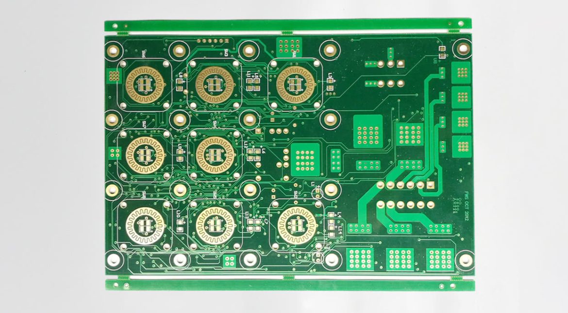
Silkscreen
The Silkscreen layer is used to print reference designators, component outlines, polarity indicators, logos, identification marks, and other information onto the PCB surface.
Silkscreen information is especially useful during PCB assembly, inspection, testing, and maintenance.
However, silkscreen design should not focus only on visual appearance. The position of text and symbols must also be considered in relation to components, pads, vias, and other conductive areas.
For example, text should not overlap solder pads because this may interfere with soldering or become partially removed during PCB manufacturing.
A good silkscreen design should follow three basic principles:
- Clear identification
- No interference with pads or components
- Easy reading during assembly and maintenance
Reference designators should remain visible whenever possible, and polarity markings should be placed in locations that can be easily identified by assembly technicians.
SMD Components
SMD Components, or surface-mount devices, are widely used in modern electronic products because they allow components to be mounted directly onto the PCB surface.
Compared with traditional through-hole components, SMD components generally require less board space and support higher component density.
Because SMD packages can be extremely small, their PCB footprints must be designed with high accuracy. Component orientation, pad dimensions, spacing, solder paste openings, and assembly tolerances all need to be considered.
For some SMD packages, the component identification and reference markings must be placed carefully to avoid interfering with the component body or soldering area.
As component sizes continue to decrease, accurate footprint design becomes increasingly important for reliable PCB assembly.
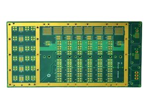
Copper Pour and Filled Copper Areas
PCB design software commonly provides different methods for creating large copper areas.
A copper pour or polygon area can be used to create a large conductive region for power distribution, grounding, heat dissipation, or electromagnetic shielding.
In some applications, a hatched or grid-style copper area may be used instead of a completely solid copper region.
The choice between a solid copper area and a grid-style copper structure depends on the electrical, thermal, mechanical, and manufacturing requirements of the PCB.
For high-current power distribution and grounding, solid copper areas are generally preferred when the design permits them.
Copper areas can also reduce the effective impedance of power and ground paths and help improve overall signal integrity.
Solder Mask
The Solder Mask is a protective coating applied to the PCB surface.
It covers most exposed copper areas while leaving specific regions, such as solder pads, exposed for component soldering.
The solder mask provides several important functions:
- Prevents accidental solder bridges
- Protects exposed copper from oxidation
- Improves electrical insulation
- Helps prevent contamination
- Defines the areas available for soldering
Solder mask openings should be designed according to the requirements of the PCB manufacturing and assembly processes.
The relationship between the solder mask opening and the pad size is particularly important for fine-pitch SMD components.
Incorrect solder mask settings may result in insufficient pad exposure, soldering defects, or unintended copper exposure.
Fly Lines
Fly Lines are temporary visual connections used during PCB layout to indicate electrical connections that still need to be routed.
After the schematic netlist is imported into the PCB design software and components are placed, fly lines help designers understand the relationships between different components.
They are particularly useful during component placement because designers can observe how many connections cross between different areas of the PCB.
A good placement strategy attempts to minimize unnecessary fly-line crossings before routing begins.
This is especially important for automated routing. Better component placement can significantly improve the efficiency and completion rate of automatic routing.
After routing is completed, remaining fly lines can also be used to identify nets that have not yet been connected.
Any remaining unconnected nets should be carefully investigated before manufacturing. Designers can then modify the routing or adjust the PCB layout to complete the required electrical connections.
In certain special situations, a zero-ohm resistor may be used as a jumper to connect two points when direct routing is impractical. However, this approach should be used carefully because it increases component count and may affect assembly cost and board space.
Conclusion
Understanding PCB Design fundamentals is essential for producing reliable and manufacturable circuit boards.
Correct management of PCB Layers, proper Via design, accurate PCB Pads, clear Silkscreen, optimized SMD Components footprints, appropriate Solder Mask settings, and effective use of Fly Lines all contribute to a successful PCB layout.
For modern high-density circuit boards, PCB design is no longer simply about connecting electrical nets. Designers must also consider signal integrity, power distribution, thermal management, manufacturing tolerances, assembly requirements, and long-term product reliability.
Kingda recommends integrating design-for-manufacturing and design-for-assembly considerations into the PCB design process from the beginning. By optimizing the layout and manufacturing parameters at an early stage, designers can reduce production defects, improve assembly efficiency, and achieve more reliable PCB products.