Automotive PCB Manufacturing: Process, Standards and Materials
Automotive PCB manufacturing is a specialized fabrication process governed by IPC-6012F Class 3/A requirements, IATF 16949 quality management, and AEC-Q component qualification standards. The process transforms copper-clad laminates into high-reliability circuit boards capable of withstanding -40°C to +150°C temperature extremes, high vibration, humidity, and chemical exposure for 15+ years of service life.[reference:0] Unlike consumer-grade PCBs, automotive boards require zero-defect reliability (PPM < 50)[reference:1], rigorous Interconnect Stress Testing (IST) with minimum 500 cycles[reference:2], and mandatory traceability through every manufacturing step. This guide walks through the complete automotive PCB manufacturing process—from material selection and inner layer fabrication to lamination, drilling, plating, and the extensive reliability testing that separates automotive-grade from commercial-grade boards.
What Is an Automotive PCB?
An automotive PCB is a printed circuit board designed, manufactured, and tested to meet the rigorous reliability requirements of automotive applications—engine control units (ECUs), advanced driver-assistance systems (ADAS), battery management systems (BMS), infotainment, and power electronics in electric vehicles.[reference:3] These boards must survive extreme temperature cycling (-40°C to +125°C for Grade 1, -40°C to +150°C for Grade 0),[reference:4] sustained vibration, high humidity, and chemical exposure throughout a vehicle’s 15+ year service life.[reference:5]
Key characteristics: high reliability, wide operating temperature range, IATF 16949-certified manufacturing,[reference:6] IPC-6012F Class 3/A compliance,[reference:7] AEC-Q100/Q200 component qualification,[reference:8] and mandatory 100% electrical testing. Automotive PCBs typically range from 4 to 20+ layers, with high-density interconnect (HDI) and microvia structures common in ADAS radar and camera modules.[reference:9]
For projects requiring automotive-grade PCB assembly, explore our turnkey PCB assembly services.
Automotive PCB Standards: IPC-6012F, AEC-Q and IATF 16949
Automotive PCB manufacturing is governed by a layered system of standards: a bare-board qualification spec (IPC-6012 and its automotive addendum), a component-level qualification spec (AEC-Q100/Q200), and a quality-management framework (IATF 16949).[reference:10] None of the three alone makes a board road-ready—engineers who only check one are the ones who get surprised by a field return three years into a vehicle’s life.[reference:11]
IPC-6012F and the Automotive Addendum (IPC-6012FA)
The IPC officially released IPC-6012F in Q1 2026—the most significant tightening of automotive PCB reliability requirements in over a decade.[reference:12] Key changes include: via reliability acceptance tightened from 10% to 5% maximum resistance change after thermal cycling;[reference:13] minimum copper thickness in via barrels increased from 25 µm to 28 µm for Class 3/A;[reference:14] IST (Interconnect Stress Test) elevated from optional to mandatory with minimum 500 cycles (up from 300);[reference:15] and stacked microvias now requiring qualification at the stack level, not just single-via.[reference:16] The current automotive addendum pairing is IPC-6012F plus IPC-6012FA (released December 2025).[reference:17]
AEC-Q Standards (Component Qualification)
AEC-Q100 qualifies integrated circuits (ICs) for automotive use through stress testing: 1,000 hours of High-Temperature Operating Life (HTOL) at the grade’s maximum ambient temperature—150°C for Grade 0, 125°C for Grade 1, 105°C for Grade 2, and 85°C for Grade 3.[reference:18] AEC-Q200 qualifies passive components—resistors, capacitors, inductors, and fuses.[reference:19] AEC-Q applies to components mounted on the PCB, not the bare board itself—a common misconception.[reference:20]
IATF 16949 (Quality Management)
IATF 16949 is the quality management system standard for automotive suppliers, required by all major OEMs (Toyota, VW, GM, Ford).[reference:21] PCB manufacturers serving automotive must be IATF 16949 certified, with process control, traceability, corrective actions, and continuous improvement embedded in every production step.[reference:22]
Material Selection for Automotive PCBs
Material selection is the foundation of automotive PCB reliability. The substrate must withstand extreme temperatures, humidity, and voltage bias without degradation.
Substrate Materials
High-Tg FR-4 (Tg ≥ 170°C) is the industry standard for automotive applications.[reference:23][reference:24] Standard FR-4 (Tg ~130-140°C) softens and expands dramatically in the Z-axis above its Tg, creating stress on plated through-holes that can cause barrel cracking.[reference:25][reference:26] High-Tg FR-4 offers: Tg of 170-180°C, Td (decomposition temperature) of ~340°C, lower Z-axis CTE, and reduced warpage.[reference:27] For extreme under-hood and EV power applications, ultra-high-Tg materials like Nanya NPG-190BH (Tg 190°C, Td 390°C) provide additional thermal safety margin.[reference:28][reference:29]
Key substrate requirements: CAF (Conductive Anodic Filament) resistance—must pass CAF testing at 85°C/85%RH with voltage bias, no failures allowed.[reference:30] Halogen-free compliance is required by many OEMs.[reference:31] Low Z-axis CTE prevents via barrel cracking during thermal cycling.[reference:32]
Copper and Plating
Minimum copper plating in via barrels: 25 µm (IPC Class 3 minimum), increased to 28 µm for IPC-6012F Class 3/A.[reference:33][reference:34] Heavy copper (2 oz or more) is required for power electronics in EV/HEV battery management and motor drives.[reference:35] For high-frequency ADAS applications (radar, lidar), RTF (Reverse Treated Foil) or VLP (Very Low Profile) copper is specified to minimize signal loss.[reference:36]
Surface Finishes
ENIG (Electroless Nickel Immersion Gold) is the most popular automotive finish—long shelf life, fine-pitch compatible, and excellent solderability.[reference:37] ENEPIG is used for wire bonding applications (sensors, power modules).[reference:38] OSP is only suitable if assembly occurs within days of fabrication.[reference:39]
Automotive PCB Manufacturing Process: Step-by-Step
Automotive PCB manufacturing follows a sequential fabrication process with additional quality controls at every stage to achieve near-zero defect targets (PPM < 50).[reference:40]
1. Material Preparation and Incoming Inspection
All raw materials—laminates, prepregs, copper foils, and chemicals—must have full traceability with batch/lot records. Incoming inspection verifies material certifications, Tg, Td, and CTE against specifications.[reference:41]
2. Inner Layer Fabrication
Copper-clad cores are cleaned, laminated with photoresist, exposed (using Laser Direct Imaging for fine features), developed, and etched. Automated Optical Inspection (AOI) is performed on every inner layer to detect shorts, opens, and defects—100% inspection is mandatory for automotive.[reference:42]
3. Lamination and Layer Stack-Up
Oxide treatment (brown/black oxide) roughens copper surfaces for resin bonding.[reference:43] Inner layers, prepregs, and outer copper foils are precisely aligned and laminated under heat and pressure. Lamination parameters for automotive FR-4: 180-200°C at 300-500 PSI. Post-lamination X-ray inspection verifies layer-to-layer registration—automotive Class 3/A requires tighter tolerances than commercial Class 2.[reference:44]
4. Drilling
X-ray alignment locates internal reference points before drilling. High-speed mechanical drills create through-holes; laser drilling creates microvias for HDI structures. Automotive HDI requires microvias with diameter ≤ 150 µm.[reference:45] Desmear removes resin from hole walls before plating.[reference:46]
5. Copper Plating (PTH)
Electroless copper deposition followed by electrolytic copper plating builds up the required copper thickness in via barrels. For IPC-6012F Class 3/A, minimum barrel copper thickness is 28 µm.[reference:47] Plating thickness is verified by microsection analysis on every production lot.
6. Outer Layer Imaging and Etching
Outer copper layers are patterned using the same photolithography process as inner layers. Additional copper plating may be applied to circuit areas for current-carrying capacity. 100% AOI inspection is performed on outer layers.[reference:48]
7. Solder Mask and Silkscreen
Solder mask (typically green) is applied to protect traces and prevent solder bridging. Automotive solder mask must have consistent thickness and adhesion to withstand thermal cycling without cracking.[reference:49] Silkscreen prints component designators and polarity markers.
8. Surface Finish
The specified surface finish—typically ENIG for automotive—is applied to exposed copper pads to ensure solderability and prevent oxidation.[reference:50]
9. Electrical Testing
100% electrical testing is mandatory for automotive PCBs. Flying probe testing verifies continuity and isolation for every net. For high-volume production, fixture-based testing is used.[reference:51]
10. Profiling, Inspection, and Packaging
Boards are routed from the panel, final visual inspection is performed, and boards are vacuum-packed with desiccant and humidity indicators. Full traceability—each board is marked with a unique identifier (laser-marked 2D barcode) linking to production records.[reference:52]
For prototyping and low-volume automotive PCB needs, explore our prototype PCB assembly services.
Reliability Testing for Automotive PCBs
Automotive PCB reliability testing goes far beyond standard commercial board testing. The following tests are required for automotive qualification:
Interconnect Stress Testing (IST)
IST is now mandatory for IPC-6012F Class 3/A—previously optional.[reference:53] Minimum 500 cycles to failure (up from 300).[reference:54] Failure defined as resistance increase >5% (tightened from 10%) or any single cycle resistance spike >15%.[reference:55]
Thermal Cycling
Boards are cycled from -40°C to +125°C for 1,000-2,000 cycles.[reference:56] Acceptance: no resistance increase >10% after cycling.[reference:57]
CAF Testing
Conductive Anodic Filament testing: boards held at 85°C/85%RH with voltage bias (50-100 VDC) for 500-1,000 hours.[reference:58] Insulation resistance between conductors is monitored—no failures allowed.[reference:59]
Cleanliness Testing
Ionic contamination must be <1.56 µg NaCl/cm² (IPC standard); many OEMs require <0.75 µg NaCl/cm².[reference:60] ROSE testing or ion chromatography is performed to prevent electrochemical migration.[reference:61]
Design Considerations for Automotive Applications
Designing for automotive PCBs requires specific considerations beyond standard PCB design:
Vibration Resistance
Avoid large, heavy through-hole components on single mounting points.[reference:62] Use wide traces and ample annular ring copper.[reference:63] Use stiffening brackets for large connectors.[reference:64] Apply conformal coating to prevent fatigue cracks.[reference:65]
Thermal Management
Automotive temperature ranges are extreme—plan thermal paths from the start.[reference:66] Place thermal vias under power components.[reference:67] Consider aluminum-based MCPCB for LED and power applications.[reference:68]
Traceability
Every board must have a unique identifier (laser-marked 2D barcode).[reference:69] Complete material batch traceability is required.[reference:70] Process parameters for every production run must be recorded.[reference:71] Most OEMs require 15+ years of record retention.[reference:72]
Component Selection
All components must meet AEC-Q100 (ICs) or AEC-Q200 (passives) qualification.[reference:73][reference:74] Temperature grade must match the vehicle zone: Grade 0 (-40°C to +150°C) for under-hood/powertrain; Grade 1 (-40°C to +125°C) for engine compartment; Grade 2 (-40°C to +105°C) for passenger compartment.[reference:75]
For expert DFM support on your automotive PCB design, explore our PCB design and layout services.
Common Manufacturing Challenges and Solutions
Automotive PCB manufacturing presents unique challenges that require specialized process control:
Thermal Cycling-Induced Via Failure
Problem: Copper expands at ~17 ppm/°C; standard FR-4 expands much more in the Z-axis above Tg.[reference:76] This mismatch causes barrel cracking and opens after extended thermal cycling.
Solution: Specify High-Tg FR-4 (≥170°C) with low Z-axis CTE.[reference:77] Ensure minimum barrel copper thickness of 28 µm for Class 3/A.[reference:78]
CAF (Conductive Anodic Filament) Growth
Problem: Copper migration along glass fibers under voltage bias and humidity creates conductive filaments that short adjacent conductors.
Solution: Use CAF-resistant laminates.[reference:79] Maintain tight process control on drilling and desmear to prevent resin voids.[reference:80]
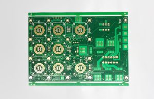
Microvia Reliability in HDI Designs
Problem: Stacked microvias in radar and lidar controllers can delaminate under extended thermal cycling—structures that passed single-via testing failed at stack level.[reference:81]
Solution: IPC-6012F now requires qualification at the stack level, not just single-via.[reference:82]
Registration Accuracy
Problem: High layer counts (10-20+ layers) in automotive ECUs require extremely tight layer-to-layer registration—misalignment causes opens when drilled holes miss internal pads.
Solution: Use Laser Direct Imaging (LDI) for exposure, apply proper scaling compensation, and perform X-ray alignment before drilling.
Frequently Asked Questions
What is the difference between automotive-grade and commercial-grade PCBs?
Automotive-grade PCBs must survive -40°C to +150°C temperature extremes, 15+ years of service life, and rigorous vibration/humidity/chemical exposure.[reference:83] They require IATF 16949-certified manufacturing,[reference:84] IPC-6012F Class 3/A compliance,[reference:85] AEC-Q qualified components,[reference:86] 100% electrical testing, and full traceability—commercial PCBs have none of these requirements. Cost is typically 30-100% higher.[reference:87]
What is the standard tolerance for automotive PCB manufacturing?
Automotive PCBs follow IPC-6012F Class 3/A tolerances. Minimum trace/space: 3/3 mil (75/75 µm) with contact printing, 2/2 mil (50/50 µm) with LDI. Layer-to-layer registration: ±2 mil (50 µm) for Class 3/A. Minimum via barrel copper: 28 µm for Class 3/A.[reference:88]
What materials are used in automotive PCB manufacturing?
High-Tg FR-4 (Tg ≥ 170°C) is the standard substrate for most automotive applications.[reference:89][reference:90] For extreme under-hood and EV power, ultra-high-Tg materials like Nanya NPG-190BH (Tg 190°C) are specified.[reference:91] Surface finish is typically ENIG.[reference:92]
What is the difference between AEC-Q100 and IPC-6012F?
AEC-Q100 qualifies the ICs (active components) mounted on the board—it does NOT cover the bare PCB itself.[reference:93] IPC-6012F qualifies the bare PCB fabrication—materials, plating, lamination, drilling, and reliability testing.[reference:94] Both are required for a complete automotive-grade solution.[reference:95]
What is IST testing and why is it important for automotive PCBs?
IST (Interconnect Stress Test) is a rapid thermal cycling test that stresses via structures to verify long-term reliability.[reference:96] Under IPC-6012F, IST is now mandatory for Class 3/A with minimum 500 cycles (up from 300).[reference:97] Failure defined as >5% resistance increase.[reference:98]
Why is High-Tg FR-4 required for automotive PCBs?
Standard FR-4 (Tg 130-140°C) softens and expands dramatically above its Tg, creating stress on plated through-holes that causes barrel cracking.[reference:99] High-Tg FR-4 (Tg ≥ 170°C) maintains structural rigidity at higher temperatures, with lower Z-axis CTE and reduced warpage.[reference:100]
Need an Automotive PCB Manufacturing Partner?
At gopcb, we specialize in high-reliability automotive PCB manufacturing with IATF 16949 process controls and IPC-6012F Class 3/A compliance. Our engineering team provides free DFM analysis to ensure your design is optimized for automotive-grade reliability.
References
- [Standard] IPC-6012F. (2026). Qualification and Performance Specification for Rigid Printed Boards.
- [Standard] IPC-6012FA. Automotive Applications Addendum to IPC-6012F.
- [Standard] AEC-Q100. Failure Mechanism Based Stress Test Qualification for Integrated Circuits.
- [Standard] AEC-Q200. Stress Test Qualification for Passive Components.
- [Standard] IATF 16949. Quality Management System for Automotive Suppliers.
- [Industry Report] AtlasPCB. (2026). IPC Releases Updated IPC-6012F Standard with Stricter Reliability Requirements for Automotive PCBs.
- [Industry Guide] NextPCB. (2026). Automotive PCB Design: IPC-6012DA, AEC-Q200 and What Makes Car-Grade Boards Different.
- [Industry Guide] AtlasPCB. (2026). Automotive PCB Requirements: AEC-Q Standards, IATF 16949, Temperature Grades, and Material Selection.
- [Industry Guide] JLCPCB. (2026). Why High Tg FR4 Is the Smart Choice for Reliable High-Temperature PCBs.
- [Manufacturer Data] PCBSync. (2026). Nanya NPG-190BH Automotive Laminate: Ultra-High-Tg Reliability for Next-Gen Vehicles.
All references are provided for informational purposes. gopcb is not affiliated with any third-party sites listed.