PCB Decoupling Capacitor Placement and Installation Guide
Proper power distribution is essential for achieving stable and reliable electronic circuit performance. During high-speed switching, digital ICs can generate short-duration current spikes that cause power supply voltage fluctuations, electromagnetic interference, and signal integrity problems.
Using PCB decoupling capacitors correctly is one of the most effective ways to suppress these disturbances. However, simply adding capacitors to a circuit board is not enough. Capacitor value, frequency characteristics, placement, current-loop area, via configuration, and parasitic inductance all affect the effectiveness of the decoupling network.
This guide explains the causes of spike currents and provides practical recommendations for PCB layout, capacitor selection, placement, and installation.
How Do Spike Currents Form?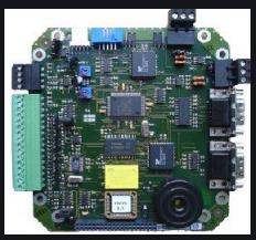
When a digital circuit switches between logic states, the current drawn from the power supply can change rapidly. The current flowing when an output is driven high can differ significantly from the current flowing when the output is driven low.
During a fast transition, a temporary current spike may occur. The actual power-supply current waveform can therefore contain a short-duration, high-amplitude pulse rather than changing smoothly.
The characteristics of this spike current depend on several factors, including:
- The semiconductor technology used by the IC
- Switching speed
- Output load capacitance
- Interconnect parasitics
- Power distribution network impedance
- PCB trace and plane geometry
In modern high-speed electronics, controlling these transient currents is an important part of power integrity design.
Main Causes of Spike Currents
Simultaneous Conduction in the Output Stage
During the transition of a digital gate, transistors in the output stage may briefly conduct simultaneously.
For example, when a logic output changes state, one transistor may not have completely turned off before the complementary transistor begins conducting. During this short transition interval, a relatively large transient current can flow through the power supply.
Although modern logic families are designed to minimize this effect, switching transients remain an important consideration in high-speed digital circuits.
Load Capacitance
Another important source of transient current is the capacitance connected to the output of a digital device.
When an output changes from low to high, the output stage must charge the load capacitance. The charging current is supplied through the power network and can produce a temporary current spike.
When the output changes from high to low, the stored energy in the load capacitor is discharged through the output stage. Because this discharge current does not necessarily flow through the same power-supply path, its influence on the supply current can be different.
How to Suppress Spike Currents
Several design methods can be used to reduce the effects of transient currents.
1. Minimize Unnecessary Parasitic Capacitance
PCB routing should be designed to minimize unnecessary trace length and stray capacitance.
Long traces and excessive routing can increase parasitic effects and make high-speed signal transitions more difficult to control.
A well-designed PCB layout should therefore keep critical signal paths short and use appropriate reference planes to provide predictable return-current paths.
2. Reduce Power Distribution Network Impedance
A high-impedance power distribution network converts transient current into larger voltage fluctuations.
Reducing the impedance of the power network helps prevent voltage drops when an IC suddenly demands current.
Practical techniques include:
- Using solid power and ground planes
- Keeping power connections short
- Using sufficiently wide traces
- Minimizing unnecessary vias
- Providing short return-current paths
- Placing decoupling capacitors close to IC power pins
For complex boards, professional PCB manufacturing and engineering review can also help ensure that the selected layer stack-up and fabrication structure support the required electrical performance.
3. Use Properly Selected Decoupling Capacitors
A common solution is to place bulk and high-frequency capacitors at appropriate locations throughout the PCB.
A larger capacitor, such as a few microfarads, can help stabilize relatively low-frequency power fluctuations. Smaller ceramic capacitors are typically used close to IC power pins to handle high-frequency transient currents.
Typical values may include:
- 1–10 µF for local bulk decoupling
- 0.1 µF for general high-frequency decoupling
- 0.01 µF for higher-frequency noise suppression where appropriate
However, capacitor selection should not rely solely on capacitance value.
The capacitor’s ESR, ESL, package size, mounting structure, dielectric characteristics, and self-resonant frequency all influence its actual high-frequency performance.
How to Select a Decoupling Capacitor
A simplified rule sometimes used for initial capacitor selection is:
C ≈ 1/F
where:
- C is the capacitance
- F is the relevant frequency
For example:
- At 10 MHz, approximately 0.1 µF may be considered
- At 100 MHz, approximately 0.01 µF may be considered
This is only a starting point rather than a universal design rule. Modern PCB power integrity design should consider the actual transient-current spectrum, capacitor impedance curve, target impedance, and power distribution network.
The most important objective is to select a capacitor whose impedance is sufficiently low over the frequency range where the circuit requires effective current delivery.
Why Capacitor Placement Matters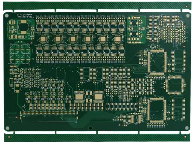
The location of a decoupling capacitor is often more important than simply increasing its capacitance.
A capacitor placed close to an IC power pin can provide a short local current path when the device suddenly demands current.
When the capacitor is placed too far away, the connecting traces and vias introduce additional inductance. At high frequencies, this parasitic inductance can significantly reduce the effectiveness of the capacitor.
This is why decoupling capacitor placement should always be considered as part of the complete current-loop design.
For high-performance electronic products, the transition from design to production should also be carefully controlled. Professional PCB assembly services can help ensure that component placement, soldering, and assembly requirements are consistent with the original design.
ESR, ESL, and Self-Resonant Frequency
An ideal capacitor would have only capacitance. A real capacitor, however, contains parasitic resistance and inductance.
These parameters are commonly represented as:
- ESR — Equivalent Series Resistance
- ESL — Equivalent Series Inductance
As a result, a real capacitor behaves approximately like a series RLC network.
Its self-resonant frequency is determined by its capacitance and parasitic inductance:
f₀ = 1 / (2π√LC)
Below the self-resonant frequency, the capacitor primarily exhibits capacitive behavior.
Near the self-resonant frequency, its impedance reaches a minimum.
Above the self-resonant frequency, parasitic inductance becomes dominant and the component increasingly behaves inductively.
This explains why simply choosing a capacitor with a larger capacitance does not necessarily improve high-frequency noise suppression.
Why Large Capacitors Cannot Replace Small High-Frequency Capacitors
A large electrolytic capacitor may provide excellent low-frequency filtering, but its relatively large package and parasitic inductance limit its effectiveness at very high frequencies.
For example, a 10 µF electrolytic capacitor may be useful for low-frequency power fluctuations, but it cannot necessarily provide an effective low-impedance path for high-frequency switching currents.
Therefore, practical power networks often use a combination of capacitors with different values and physical characteristics.
The goal is not to maximize capacitance. The goal is to minimize power-network impedance over the required frequency range.
Using an excessive number of large capacitors can also create unwanted side effects.
During power-up or hot-plugging, large capacitances can create high inrush currents that may cause:
- Temporary supply-voltage drops
- Connector arcing
- Slow voltage rise
- Increased stress on the power supply
- Longer startup times
Capacitor selection should therefore be based on the complete power system rather than capacitance alone.
PCB Layout Guidelines for Decoupling Capacitors
Place Small Capacitors Closest to the IC
In general, smaller ceramic capacitors with higher self-resonant frequencies are placed closest to the IC power pins.
Larger capacitors can be placed slightly farther away to provide lower-frequency energy storage.
A typical arrangement may use:
- Small high-frequency ceramic capacitor — closest to the power pin
- Medium-value capacitor — slightly farther away
- Larger bulk capacitor — farther from the IC or near the local power entry point
The exact values and arrangement should be determined by the IC manufacturer’s recommendations and the target power integrity requirements.
Keep Decoupling Capacitors Close to the Power Pins
The capacitor should be positioned as close as practical to the corresponding power and ground pins.
The objective is to minimize the complete high-frequency current-loop area:
Power Plane → Via → Trace → Capacitor → Trace → Via → Ground Plane
A smaller loop area generally means lower parasitic inductance and better high-frequency performance.
Distribute Capacitors Around the Device
When an IC has multiple power and ground pins distributed around the package, decoupling should not necessarily be concentrated in one area.
Capacitors should be distributed according to the power-pin arrangement and the current paths required by the device.
Concentrating all capacitors on one side of a large IC can increase the effective distance between some power pins and their local decoupling paths.
For complex multilayer boards, careful stack-up design and power-plane planning are equally important. Advanced PCB manufacturing capabilities can support multilayer, HDI, controlled-impedance, and other complex PCB structures when the design requires them.
How to Install Decoupling Capacitors
The physical connection between the capacitor pads, vias, and power planes has a major influence on high-frequency performance.
Method 1: Long Trace From the Pad to the Via
One approach is to route a relatively long trace from the capacitor pad to a distant via.
This method should generally be avoided for high-frequency decoupling because the long trace adds unnecessary inductance and increases the current-loop area.
Method 2: Vias Close to Both Pads
A better approach is to place the power and ground vias immediately adjacent to the corresponding capacitor pads.
This significantly reduces the connection length and therefore reduces parasitic inductance.
Method 3: Vias Beside the Pads
Moving the vias even closer to the capacitor pads can further reduce the current-loop area.
This is generally a good layout technique when sufficient PCB space is available.
Method 4: Multiple Vias at Both Ends
Using multiple vias at the power and ground sides can further reduce effective inductance.
Parallel vias provide multiple current paths and can improve the high-frequency connection between the capacitor and the power or ground planes.
This method is particularly useful when the design has sufficient routing and placement space.
Method 5: Via-in-Pad
Via-in-pad can provide an extremely short electrical path between the component pad and the internal plane.
However, this approach requires appropriate PCB fabrication technology, such as controlled via filling and planarization.
Therefore, via-in-pad should only be used when the manufacturing process supports it and when the benefits justify the additional fabrication requirements.
Avoid Sharing Vias Between Multiple Decoupling Capacitors
Using one common via for several capacitors may appear to save PCB space, but it can increase the shared current path and reduce the effectiveness of high-frequency decoupling.
Where practical, each capacitor should have a short and direct connection to the appropriate power and ground planes.
Instead of simply increasing the number of capacitors, engineers should optimize the capacitor network and placement strategy.
Keep Connections Short and Wide
The connection between the capacitor pad and via should be as short and wide as practical.
Wider traces generally have lower inductance than narrow traces.
For small packages such as 0402 capacitors, the connection geometry should still be carefully optimized rather than relying on extremely narrow traces.
The objective is to maintain a compact current loop while providing a low-impedance path between the capacitor and the power distribution network.
Practical Design Checklist
Before completing the PCB layout, engineers should review the following items:
- Place high-frequency decoupling capacitors close to IC power pins.
- Keep capacitor-to-via connections short.
- Minimize the complete current-loop area.
- Use solid power and ground reference planes where appropriate.
- Avoid unnecessarily long traces between capacitors and vias.
- Avoid unnecessary shared vias.
- Use multiple vias when required to reduce inductance.
- Consider capacitor ESR and ESL.
- Consider the self-resonant frequency of each capacitor.
- Use different capacitor values when the frequency range requires it.
- Avoid excessive bulk capacitance.
- Follow the IC manufacturer’s recommended decoupling network.
- Verify power integrity for high-speed and high-current designs.
- Confirm that the selected PCB fabrication process supports advanced via structures when required.
- Consider assembly constraints during component placement.
Design and Quality Review
The checklist below summarises the production points discussed above.
- How Do Spike Currents Form: review the production data and close any deviation before the next build.
- Main Causes of Spike Currents: confirm the requirements, process settings and inspection records at first-article approval.
- How to Suppress Spike Currents: record the agreed limits and verify them again in the production lot.
- How to Select a Decoupling Capacitor: check the drawing, process sheet and inspection plan before release.
- Why Capacitor Placement Matters: treat this as a repeat-order checkpoint and keep the result with the lot record.
- ESR, ESL, and Self-Resonant Frequency: review the production data and close any deviation before the next build.
- Why Large Capacitors Cannot Replace Small High-Frequency Capacitors: confirm the requirements, process settings and inspection records at first-article approval.
- PCB Layout Guidelines for Decoupling Capacitors: record the agreed limits and verify them again in the production lot.
Conclusion
Effective decoupling is not simply a matter of adding more capacitors to a PCB. High-frequency performance depends on the interaction between capacitance, ESR, ESL, self-resonant frequency, PCB geometry, via configuration, power planes, and current-loop area.
The most important principle is to create the shortest and lowest-inductance path possible between the IC power pins, decoupling capacitor, and ground reference.
By applying proper PCB decoupling capacitors, optimized PCB layout, and careful decoupling capacitor placement, engineers can reduce power supply noise, suppress transient voltage fluctuations, improve signal integrity, and increase overall circuit reliability.
For projects requiring prototype development, complex multilayer boards, HDI structures, or production-scale manufacturing, working with an experienced PCB manufacturing and assembly partner can help ensure that electrical design requirements are translated into a reliable production-ready circuit board.