PCB Design Optimization: A Factory-Floor Review
PCB design is a critical yet time-consuming stage in electronic product development. Even a small design error can require engineers to inspect individual nets, components, and connections throughout the entire board, resulting in significant debugging and redesign costs.
As PCB complexity increases, modern boards may contain hundreds or even thousands of components and signal connections. Manually checking every connection is not only inefficient but can also make it difficult to identify subtle problems such as incorrect net connections, floating nodes, naming inconsistencies, or unintended shorts.
A structured PCB Design Verification process can significantly reduce these risks. By combining schematic review, simulation, layout verification, and manufacturing-oriented design checks, engineers can improve both design quality and development efficiency.
A reliable PCB Design process generally includes several key stages:
- System and circuit planning
- Schematic capture
- Schematic verification
- Component and PCB footprint verification
- PCB layout
- Routing
- Design rule checking
- Simulation and validation
- Design for Manufacturability (DFM) review
- Prototype fabrication and testing
Among these stages, schematic development and verification can require a considerable amount of engineering time, particularly for complex systems.
For a board containing hundreds or thousands of connections, manually checking every net is extremely difficult. This increases the possibility of errors being carried into the PCB layout and eventually into the manufactured board.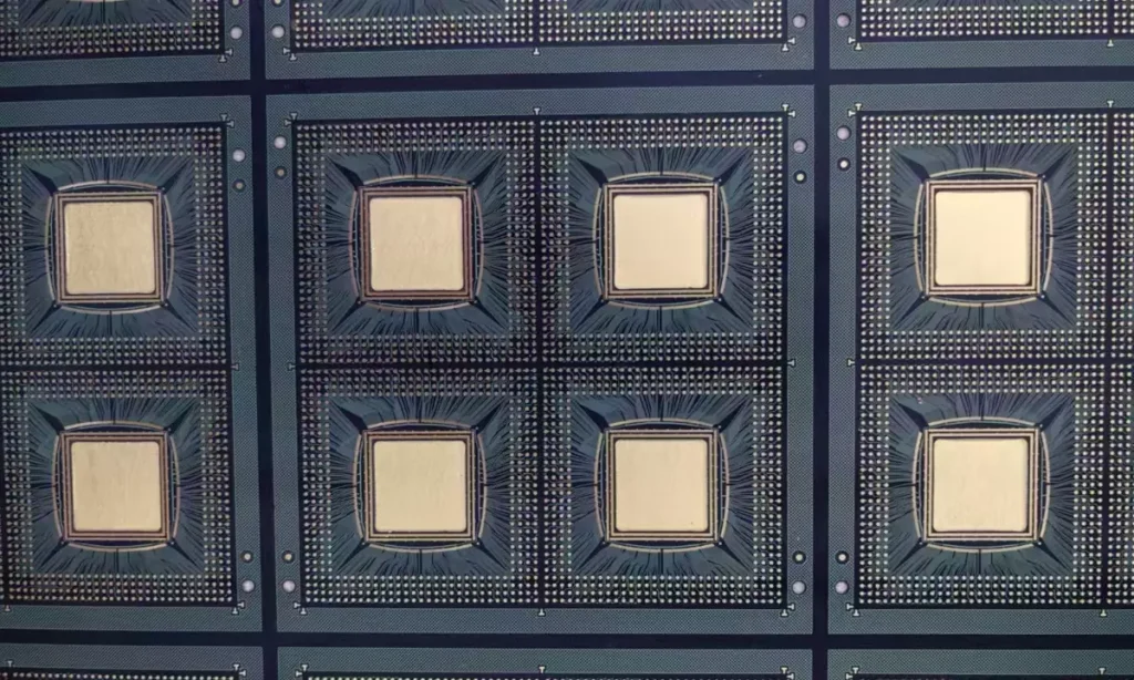
A professional PCB Layout workflow therefore requires systematic verification throughout the design process rather than relying entirely on final manual inspection.
The schematic capture stage is where many potential PCB problems originate.
Common issues include:
Similar but inconsistent net names can create unexpected connections or disconnected circuits.
For example:
- APLLVDD
- APLL_VDD
Although these names may appear similar to an engineer, PCB design software can interpret them as completely different nets depending on the naming rules of the specific software.
Signal names such as:
- VDDE
- vdde
may be treated differently by some design environments.
Engineers should establish consistent naming conventions at the beginning of the project and apply them throughout the schematic.
Simple spelling errors can create unintended or disconnected nets.
For example, a signal intended to be named:
could accidentally be entered as:
If the design software interprets these as different nets, the circuit may not function as intended.
Accidental connections between power, ground, analog, and digital signals can cause serious electrical problems.
These errors can be especially difficult to detect when the schematic becomes large and complicated.
Unconnected pins and floating nodes may cause unstable circuit behavior or prevent specific functions from operating correctly.
For this reason, PCB Schematic verification should be performed before the design is transferred to the PCB layout stage.
Consider a complex SoC-based PCB containing thousands of connections.
An engineer attempting to inspect every connection manually must repeatedly check:
- Net names
- Component pins
- Power connections
- Ground connections
- Signal paths
- Connector interfaces
- Passive components
- IC connections
- Unused pins
- Potential shorts
As the number of components and nets increases, the amount of manual verification grows rapidly.
Manual inspection is also susceptible to human error because engineers may overlook a small discrepancy after spending many hours reviewing similar connections.
Therefore, automated verification tools and simulation techniques can provide an important additional layer of protection.
One effective approach for improving PCB Design Verification is to use schematic simulation before PCB layout begins.
Schematic simulation allows engineers to evaluate circuit behavior before a physical PCB is manufactured.
A typical simulation workflow includes:
- Creating the schematic
- Building a simulation testbench
- Applying input stimulus
- Monitoring important circuit nodes
- Analyzing voltage and waveform results
- Identifying unexpected behavior
- Adjusting component values or circuit connections
- Re-running the simulation
This approach can reveal problems that may not be obvious from visual schematic inspection alone.
A testbench provides the conditions required to evaluate a circuit.
During testbench development, engineers apply appropriate excitation signals to the required inputs and monitor the circuit nodes that are important to system operation.
For example, a voltage regulator circuit can be evaluated by applying an input voltage and observing:
- Input voltage
- Output voltage
- Startup behavior
- Ripple
- Transient response
- Load response
Probes can be connected to important nodes to observe voltage levels and waveforms.
This allows engineers to compare simulated behavior against expected circuit performance.
Not every node needs to be analyzed in the same level of detail.
Engineers should prioritize:
- Power rails
- Clock signals
- Reset signals
- Analog outputs
- ADC/DAC interfaces
- High-speed interfaces
- Feedback nodes
- Control signals
Monitoring these nodes can help identify incorrect connections or unexpected circuit behavior before the PCB enters production.
The main advantage of PCB Simulation is that engineers can evaluate circuit behavior before spending time and money on PCB fabrication.
Instead of discovering an incorrect connection after receiving the prototype, engineers can identify potential problems during the schematic stage.
Simulation can help engineers investigate:
- Incorrect connections
- Unexpected voltage levels
- Incorrect component values
- Startup problems
- Signal behavior
- Power-supply performance
- Circuit stability
- Design changes
For example, if a regulator output is lower than expected during simulation, the engineer can investigate the feedback network, component values, load conditions, and connections before producing the PCB.
Simulation is not only useful for finding mistakes. It can also help engineers compare different design approaches.
Component values, input conditions, and circuit parameters can be adjusted to evaluate how the circuit responds.
For example, engineers can investigate the effect of changing: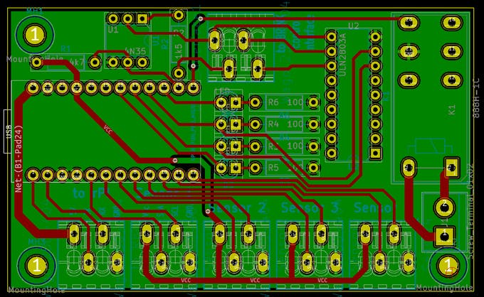
- Resistor values
- Capacitor values
- Inductor values
- Supply voltage
- Load conditions
- Input frequency
- Signal amplitude
This makes simulation a useful engineering tool for both verification and optimization.
Schematic simulation should not replace traditional PCB design checks. Instead, it should be part of a broader verification workflow.
A robust PCB Layout process should include several levels of inspection.
Check:
- Net connectivity
- Power and ground
- Component values
- Pin assignments
- Signal names
- Unused pins
- Critical interfaces
Before layout, verify that each PCB footprint corresponds correctly to the physical component.
Important parameters include:
- Pad dimensions
- Pin pitch
- Pin numbering
- Component outline
- Orientation
- Thermal pads
- Mechanical dimensions
An incorrect footprint can result in assembly failure even if the electrical schematic is correct.
During PCB layout, engineers should verify:
- Component placement
- Trace width
- Trace spacing
- Via dimensions
- Differential pairs
- Controlled impedance
- Power distribution
- Ground return paths
- High-speed signal routing
- Thermal requirements
Before releasing production files, engineers should also check whether the PCB can be manufactured according to the selected process capabilities.
Typical DFM checks include:
- Minimum trace width
- Minimum spacing
- Drill diameter
- Annular ring
- Copper thickness
- Solder mask clearance
- Board outline
- Layer stack-up
- Impedance requirements
PCB Manufacturing Capabilities
PCB development should be treated as an iterative engineering process.
Instead of completing the entire design and checking everything at the end, engineers can continuously review and improve the design throughout development.
A practical iterative process is:
Create the circuit according to the system architecture and electrical requirements.
Check connectivity, component values, power supplies, signal names, and critical interfaces.
Use PCB Simulation or circuit simulation tools to evaluate important functional blocks.
Confirm component dimensions and pad configurations before PCB layout.
Place components according to signal flow, power distribution, thermal requirements, and mechanical constraints.
Optimize critical signal paths while maintaining appropriate spacing, impedance, and return-current paths.
Use automated DRC tools to identify potential manufacturing and electrical violations.
Verify that the completed design is compatible with the intended PCB manufacturing process.
After the design passes verification, fabricate the prototype and perform electrical and functional testing.
Design for Manufacturability should be considered before production files are released.
A board that works electrically may still be difficult or expensive to manufacture if it contains unnecessarily aggressive design rules.
For example, extremely narrow traces, small drills, complex via structures, excessive dimensional tolerances, or poor copper distribution can increase manufacturing difficulty.
Early DFM analysis can help engineers identify these problems while the design is still easy to modify.
DFM and PCB Manufacturing Support
After completing the design, the PCB should undergo appropriate inspection and testing.
Depending on the board and production requirements, verification may include:
- Design Rule Checking (DRC)
- Electrical Rule Checking (ERC)
- Automated Optical Inspection (AOI)
- X-ray inspection
- Flying probe testing
- Electrical testing
- Functional testing
- Impedance testing
- Dimensional inspection
For assembled boards, additional PCBA inspection can be used to verify solder joints, component placement, and assembly quality.
The following practices can significantly improve design reliability:
Establish standardized conventions for nets, components, connectors, power rails, and functional blocks.
Pay special attention to power, ground, clocks, reset signals, high-speed interfaces, and safety-related circuits.
Automated ERC, DRC, connectivity checks, and simulation can reduce the burden of manual inspection.
Never assume that a downloaded footprint is automatically correct. Compare it with the component manufacturer’s mechanical drawing.
Define the PCB layer structure and impedance requirements before routing high-speed signals.
Check manufacturing limitations while the design is still flexible.
Maintain clear documentation for component selection, stack-up, routing rules, simulation results, and design changes.
Reducing PCB design errors requires more than simply checking traces after the layout has been completed.
A reliable development process combines PCB Design, PCB Schematic verification, simulation, optimized PCB Layout, automated design-rule checking, and DFM analysis.
By identifying problems earlier in the design cycle, engineers can reduce prototype iterations, shorten development time, lower manufacturing costs, and improve the reliability of the finished electronic product.
For increasingly complex electronic systems, PCB Simulation and systematic PCB Design Verification provide valuable tools for identifying problems before they become expensive hardware failures.
The goal is not simply to create a PCB that works, but to develop a board that is electrically reliable, manufacturable, testable, and ready for stable production.
Technical Summary
Use this short review when the design moves from quotation into production.
- A reliable PCB Design process generally includes several key stages: record the agreed limits and verify them again in the production lot.
- could accidentally be entered as: check the drawing, process sheet and inspection plan before release.
- Engineers should prioritize: treat this as a repeat-order checkpoint and keep the result with the lot record.
- Simulation can help engineers investigate: review the production data and close any deviation before the next build.
- For example, engineers can investigate the effect of changing: confirm the requirements, process settings and inspection records at first-article approval.
- During PCB layout, engineers should verify: record the agreed limits and verify them again in the production lot.
- Typical DFM checks include: check the drawing, process sheet and inspection plan before release.
- A practical iterative process is: treat this as a repeat-order checkpoint and keep the result with the lot record.