



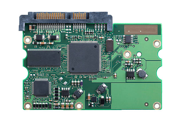
Small-Batch PCB Prototyping for Security Surveillance PCB Systems
From 24-hour urban surveillance to intelligent security systems deployed in industrial parks, modern security and surveillance equipment has become an essential part of security infrastructure. As surveillance technology continues to evolve toward higher resolution, greater intelligence, and more compact integration, the performance requirements for the PCB inside these systems are becoming increasingly demanding.
The PCB serves as the electrical platform for electronic components and signal transmission. Its design quality, manufacturing accuracy, and reliability can directly influence the performance and stability of the final surveillance product.
For security equipment manufacturers, however, developing a new PCB often involves multiple design iterations and functional tests. Producing large quantities before the design has been fully validated can increase both development costs and manufacturing risks. This is why PCB Prototyping has become an important link between an initial design concept and successful product commercialization.
Small-batch prototyping allows engineering teams to manufacture a limited number of boards, verify the actual performance of the design, identify potential problems, and optimize the solution before moving into larger-scale production.
Security surveillance equipment must often operate continuously in environments where reliability and signal quality are critical.
Typical applications include:
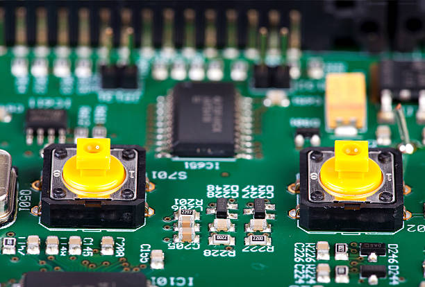
These products may require stable high-speed signal transmission, multiple electronic components, compact circuit layouts, thermal management, and resistance to environmental conditions.
During product development, engineers may need to verify whether a particular PCB layout affects signal transmission, whether selected materials are appropriate for the intended operating environment, or whether a compact component arrangement creates thermal or manufacturing problems.
Small-batch prototypes provide physical boards for these tests before the design is finalized.
A PCB that appears correct in the design environment may still encounter unexpected problems during physical testing.
For example, engineers may discover:
Identifying these issues during the prototype stage is generally more efficient than discovering them after mass production begins.
A small prototype run therefore acts as a controlled validation stage, helping engineering teams reduce design uncertainty and establish a stronger foundation for subsequent production.
The first major advantage of Rapid PCB Prototyping is the ability to validate a PCB design using physical samples.
Engineering teams can assemble prototype boards and evaluate their actual performance under realistic operating conditions. Depending on the application, testing may include signal transmission, electrical continuity, thermal behavior, component compatibility, mechanical fit, and environmental performance.
The results can then be compared with the original design requirements.
If a problem is identified, the PCB layout or manufacturing specification can be modified before production quantities increase.
This creates a practical development cycle:
Design → Prototype → Test → Optimize → Re-prototype → Production
Such a process is particularly valuable for security surveillance products where product specifications may continue to evolve during development.
The security industry is highly competitive, and product development cycles are becoming shorter.
A long prototype lead time can delay functional testing, certification, customer demonstrations, and market introduction. Rapid prototyping helps engineering teams obtain physical samples sooner and shorten the interval between design changes and verification.
For products with frequent revisions, faster prototype turnaround allows teams to complete more design iterations within the same development period.
This is especially useful when manufacturers need to respond quickly to:
During the research and development stage, manufacturers may only need several boards or a few dozen units for testing.
Committing to a large production quantity at this stage can result in unnecessary material, tooling, and manufacturing costs.
Small-batch production allows companies to manufacture according to actual development requirements. Engineers can verify the design without committing substantial resources to an unproven solution.
Once the design has passed validation, the production quantity can gradually increase.
This makes small-batch prototyping particularly suitable for startups, research teams, new product development projects, and customized surveillance equipment.
Different surveillance products require different PCB material solutions.
For conventional control circuits, standard FR-4 materials may be sufficient. However, applications involving high-speed signal transmission, high operating temperatures, compact structures, or demanding electrical performance may require higher-performance materials.
Material selection should consider:
Choosing the appropriate material at the prototype stage allows engineers to evaluate real-world performance before committing to volume production.
Modern surveillance systems increasingly use high-resolution cameras, high-speed processors, network interfaces, and other high-speed electronic components.
As signal frequencies increase, PCB layout and stack-up design become more important.
Engineers need to consider trace geometry, reference planes, return paths, layer spacing, grounding, and electromagnetic compatibility during PCB development.
For complex designs, professional PCB Design and Layout support can help evaluate high-speed, high-frequency, multilayer, HDI, impedance-controlled, and EMC requirements before fabrication. PCB Design and Layout
A well-engineered PCB layout can help reduce signal degradation and electromagnetic interference while improving overall system stability.
Security surveillance equipment is becoming smaller while integrating more functions. A single device may contain image sensors, processors, memory, communication interfaces, power management circuits, storage interfaces, and other components.
As available PCB space becomes limited, higher circuit density is often required.
An HDI PCB can use technologies such as microvias, blind vias, buried vias, fine-line routing, and sequential buildup to increase interconnection density within a smaller board area.
This can be useful for compact surveillance terminals, intelligent cameras, network security devices, and other highly integrated electronic products. HDI PCB Manufacturing
Small-batch production does not mean that quality requirements can be reduced.
Prototype boards are often used to make important engineering decisions. If prototype quality is inconsistent, engineers may receive inaccurate test results and make incorrect conclusions about the design.
Therefore, prototype manufacturing should include appropriate engineering review, material verification, process control, inspection, and electrical testing.
Typical quality-control activities may include:
A systematic quality process helps ensure that prototype boards accurately represent the intended production design.
Quality control should begin before manufacturing starts.
The PCB manufacturer should verify the final design files, material, board thickness, copper thickness, layer count, stack-up, surface finish, solder mask, and other important specifications.
During production, processes such as imaging, etching, lamination, drilling, copper plating, solder mask application, surface finishing, and electrical testing should be appropriately controlled.
A structured quality management system helps maintain consistency throughout these stages. GOPCBA’s quality management process covers design review, DFM checking, new product introduction, PCB manufacturing, testing, incoming material inspection, and production control. PCB Quality Management
The prototype stage should not be viewed simply as producing a few sample boards. It should be treated as an engineering validation stage.
The development team can use prototype boards to evaluate:
The results provide valuable feedback for PCB optimization.
Prototype manufacturing also allows engineers and manufacturers to identify potential production challenges.
For example, complex multilayer structures may require additional process optimization, while fine-line designs may require tighter control of imaging and etching.
A Multilayer PCB may be selected when the surveillance system requires more routing layers, separate power and ground structures, or higher circuit integration.
For these designs, stack-up configuration, dielectric thickness, copper thickness, layer registration, via structures, and lamination parameters should be evaluated together. Multilayer PCB Manufacturing
Once the prototype has been validated, the manufacturing process can be standardized for the next production stage.
PCB development rarely follows a completely fixed path. During testing, engineering teams may need to modify routing, change components, adjust board dimensions, or revise manufacturing specifications.
A responsive PCB manufacturing partner should be able to communicate quickly with the engineering team and evaluate these changes efficiently.
This can reduce unnecessary delays between:
Design Revision → Engineering Review → PCB Fabrication → Testing → Optimization
The quantity required by a project may change significantly throughout its development.
A typical project may progress from:
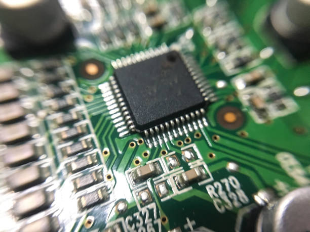
A flexible manufacturing system should therefore be able to support different production stages without compromising the key specifications established during prototype validation.
GOPCBA provides PCB manufacturing services covering prototype development, multilayer PCB fabrication, HDI, high-frequency PCB, controlled-impedance PCB, and other advanced PCB technologies. PCB Manufacturing Services
Small-batch PCB prototyping can support a wide range of security and surveillance applications.
High-resolution cameras require reliable image transmission and processing circuits. Prototype PCBs can be used to verify camera interfaces, signal integrity, power distribution, and component integration.
AI-enabled surveillance equipment may integrate processors, memory, communication interfaces, image processing circuits, and other high-density components.
Prototype testing helps engineers validate the interaction between these functional blocks before production.
Industrial monitoring systems may operate continuously in demanding environments. PCB prototypes can be evaluated for thermal performance, environmental stability, signal reliability, and mechanical compatibility.
Modern surveillance systems increasingly rely on network communication. PCB design must therefore accommodate high-speed interfaces and stable signal transmission.
Prototype testing provides an opportunity to verify these interfaces before finalizing the production design.
Small-batch PCB prototyping has become an important part of modern security surveillance product development. It allows manufacturers to validate PCB designs with physical samples, identify potential problems, optimize manufacturing processes, control development costs, and accelerate product iterations.
For increasingly sophisticated surveillance systems, PCB requirements extend beyond basic circuit connectivity. Signal integrity, electromagnetic compatibility, thermal management, circuit density, material selection, manufacturing accuracy, and quality control all need to be considered during the development process.
A structured prototype-to-production workflow enables engineering teams to test ideas quickly while reducing the risks associated with large-scale manufacturing.
By combining appropriate PCB technology, responsive engineering support, systematic quality control, and flexible production capabilities, manufacturers can move security surveillance products from initial concepts to reliable commercial solutions more efficiently.

1 Comment
Security Surveillance PCB Manufacturing for Reliable Monitoring Systems
[…] applications requiring rapid design verification or specialized security electronics, small-batch PCB prototyping for security surveillance systemscan help manufacturers validate circuit performance before moving into larger production […]