Miniaturized Medical PCB Manufacturing for Implantable Devices
Implantable medical devices are becoming smaller, smarter, and more capable. From cardiac monitoring and stimulation systems to neurostimulation and other implantable electronic platforms, engineers must integrate increasingly sophisticated electronic functions into extremely limited physical spaces.
The PCB is a critical part of this miniaturization process. Unlike conventional circuit boards, an Implantable Medical PCB may need to accommodate sensing, signal conditioning, processing, communication, and power-management functions within a highly constrained mechanical envelope.
This creates significant challenges in PCB design and manufacturing. Higher circuit density must be achieved without compromising electrical performance, interconnection reliability, mechanical integrity, or manufacturability.
As a result, modern Medical PCB Manufacturing increasingly relies on technologies such as HDI structures, microvias, fine-pitch routing, thin materials, multilayer construction, and flexible or rigid-flex configurations.
Why Miniaturization Matters in Implantable Medical Electronics
The physical size of an implantable device directly affects its mechanical design and clinical application. Reducing the size and weight of the electronics can provide engineers with greater freedom when developing compact medical systems.
However, PCB miniaturization is not simply a matter of making the board smaller.
The same circuit functions must still be maintained while available routing space decreases. Designers must therefore optimize:
- Trace width and spacing
- Pad dimensions
- Via structures
- Layer count
- Component placement
- Signal routing
- Power distribution
- Ground structures
- Thermal considerations
- Mechanical integration
The goal is to achieve higher functional density while maintaining an appropriate reliability margin.
Key Manufacturing Challenges for Miniaturized Medical PCBs
Extremely Limited PCB Space
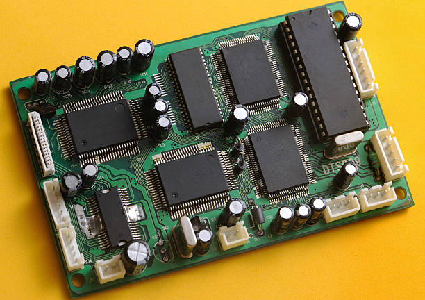
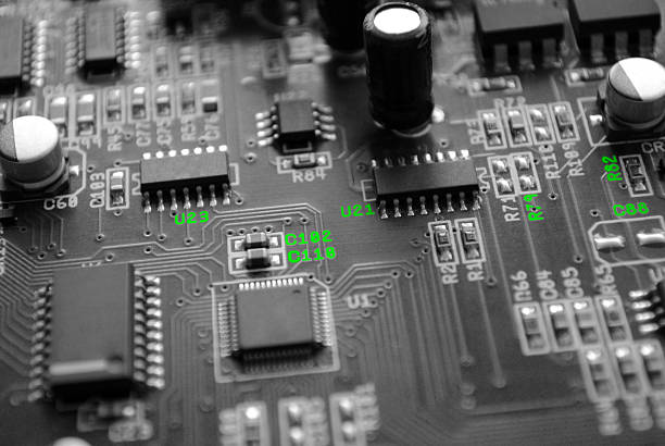
A conventional PCB design may have sufficient area for components, routing, connectors, and test structures. Implantable electronics often have much less available space.
This makes traditional routing approaches increasingly inefficient.
An advanced Miniaturized Medical PCB may require fine-line routing, smaller vias, sequential build-up structures, and high-density component placement to fit the required circuit into the available area.
The manufacturing process must therefore maintain tight control over dimensional accuracy and registration between layers.
Fine-Line and Fine-Pitch Manufacturing
As board dimensions decrease, circuit density increases. Fine-line and fine-space structures allow more electrical connections to be placed within a limited PCB area.
However, smaller features also reduce manufacturing margins.
Small variations in imaging, etching, lamination, drilling, or registration can have a greater impact on the finished circuit.
For this reason, miniaturized PCB production requires a manufacturing process capable of maintaining consistent line geometry, pad dimensions, via structures, and layer alignment.
HDI Technology for Implantable Medical PCBs
High-Density Interconnect technology is one of the most important technologies for compact electronic products.
An HDI Medical PCB uses structures such as microvias, blind vias, fine lines, small pads, and sequential lamination to create more efficient electrical interconnections.
Compared with conventional multilayer construction, HDI can provide:
- Higher wiring density
- Shorter electrical paths
- More efficient use of PCB space
- Smaller via structures
- Greater component-placement flexibility
- Better support for compact electronic packaging
GOPCBA’s published HDI capabilities include fine-line structures, microvias, blind and buried vias, copper-filled microvias, and sequential build-up structures for high-density electronic applications.
For implantable or other highly miniaturized medical electronics, however, the appropriate HDI structure should be determined according to the device’s electrical, mechanical, manufacturing, and reliability requirements.
Microvias and High-Density Interconnections
Microvias are particularly valuable when PCB space is limited.
Unlike conventional through-hole vias that pass through multiple PCB layers, microvias can connect specific layers within a build-up structure. This allows designers to use routing space more efficiently.
Advantages of Microvia Structures
Depending on the design, microvias can help:
- Reduce via footprint
- Increase routing density
- Support fine-pitch components
- Shorten interconnection paths
- Improve layer-to-layer connectivity
- Enable compact component placement
Microvia reliability is highly dependent on material selection, aspect ratio, laser-drilling quality, copper plating, filling processes, and thermal/mechanical design.
For this reason, microvia design should be evaluated together with the manufacturer’s actual production capability rather than specified only from a theoretical minimum feature size.
Material Selection for Miniaturized Medical PCBs
Material selection becomes increasingly important as PCB dimensions and feature sizes decrease.
Depending on the application, designers may consider materials such as medical-grade FR-4, polyimide-based flexible materials, high-TG laminates, and specialized substrates.
The appropriate material should be selected based on the actual electrical, mechanical, thermal, environmental, and packaging requirements.
Important Material Considerations
Engineers may evaluate:
- Dielectric performance
- Dimensional stability
- Thermal expansion
- Mechanical strength
- Moisture resistance
- Flexibility
- Operating temperature
- Layer thickness
- Copper adhesion
- Long-term reliability
For some highly specialized implantable applications, the PCB may also need to be integrated into a hermetic or otherwise protected package.
It is important to distinguish the PCB material from the complete implantable medical device. Biocompatibility, sterilization compatibility, body-contact requirements, and long-term biological safety must be evaluated at the finished-device and material-system level according to the applicable design and regulatory requirements.
Flexible and Rigid-Flex PCB Solutions
Not every implantable medical device is best served by a conventional rigid PCB.
When electronic circuits need to follow a curved or constrained mechanical structure, flexible or rigid-flex PCB technology can provide additional design freedom.
A Rigid-Flex Medical PCB combines rigid PCB sections with flexible circuit sections within one integrated structure.
This can help reduce:
- Connectors
- Cables
- Wiring interfaces
- Assembly space
- Interconnection points
GOPCBA’s rigid-flex manufacturing information identifies medical electronics as one of the applications where rigid-flex technology can help achieve compact mechanical integration and reduce conventional cable and connector requirements.
For implantable applications, the flexible structure must still be designed according to bend radius, copper construction, layer count, mechanical stress, and the intended packaging environment.
Signal Integrity in Miniaturized Implantable PCBs
Miniaturization should never come at the expense of signal quality.
Implantable medical electronics may process low-level sensor signals, stimulation signals, digital data, or wireless communication signals. As traces become closer together and routing becomes denser, engineers must carefully manage unwanted coupling and electrical noise.
Important design considerations include:
Analog Signal Routing
Sensitive analog signals should be routed away from major noise sources whenever practical.
Designers may consider:
- Short signal paths
- Appropriate grounding
- Power filtering
- Separation of analog and digital sections
- Controlled return-current paths
- Guarding or shielding where appropriate
High-Speed Digital Signals
Where high-speed interfaces are present, controlled impedance and differential-pair routing may be required.
The stack-up, dielectric thickness, copper geometry, trace width, spacing, and reference-plane structure should be considered together to achieve the required electrical characteristics.
GOPCBA’s medical PCB manufacturing capabilities include controlled-impedance and high-density PCB technologies for applications requiring stable electrical performance.
Precision Manufacturing and Process Control
The smaller the PCB feature, the more significant manufacturing variation becomes.
For miniaturized medical electronics, production control should cover the entire manufacturing chain.
Imaging and Etching
Circuit imaging must accurately transfer the design data onto the copper surface.
Etching then defines the final conductor geometry. Excessive or insufficient etching can alter trace width and spacing, which may affect electrical and manufacturing performance.
Laser Drilling
For HDI structures, laser drilling is used to create microvias.
Drilling accuracy, hole geometry, material interaction, and subsequent copper plating all influence the reliability of the finished interconnection.
Lamination and Layer Registration
Multilayer and HDI boards require accurate registration between individual layers.
As feature sizes become smaller, even relatively small registration errors can affect pads, vias, traces, and component connections.
Controlled lamination parameters are therefore essential for maintaining dimensional stability and interlayer alignment.
Quality Control for Implantable Medical PCB Manufacturing
Reliability requirements for implantable electronics can be exceptionally demanding because the final system may be difficult or impossible to access after implantation.
This makes manufacturing consistency particularly important.
A comprehensive quality-control process may include:
- Incoming material inspection
- Material traceability
- DFM review
- Dimensional inspection
- AOI
- X-ray inspection
- Electrical continuity testing
- Insulation testing
- Microvia inspection
- Cross-section analysis
- Assembly inspection
- Functional testing
The exact inspection and validation requirements should be established according to the finished device, customer specifications, applicable standards, and risk-management process.
GOPCBA provides PCB fabrication, component sourcing, SMT/THT assembly, inspection, testing, and engineering support as part of its integrated manufacturing workflow.
Traceability and Manufacturing Documentation
For high-reliability medical electronics, quality is not limited to the physical PCB.
Manufacturing records can be important for understanding how a specific board or assembly was produced.
Depending on the project, traceability may cover:
- Raw material batches
- PCB production records
- Component lot information
- Assembly parameters
- Inspection results
- Electrical test results
- Functional test data
- Manufacturing revisions
This information can support production consistency, engineering investigations, corrective actions, and controlled product changes.
PCB Assembly for Miniaturized Medical Devices
Miniaturized PCB fabrication and component assembly must be considered together.
As PCB dimensions decrease, component packages may become smaller and component spacing tighter. This increases the importance of solder-paste printing, component placement accuracy, reflow control, and inspection.
Modern medical PCB assembly may involve:
- Fine-pitch SMT
- Micro-BGA
- CSP
- High-density component placement
- Mixed SMT/THT assembly
- Automated optical inspection
- X-ray inspection
- Electrical testing
GOPCBA’s published PCBA capabilities include fine-pitch component assembly, SMT, THT, SPI, AOI/AXI, and high-precision component placement.
For highly miniaturized medical electronics, PCB fabrication and assembly should therefore be developed as a coordinated process rather than as two independent manufacturing steps.
Supporting the Development of Advanced Implantable Electronics
As implantable medical systems become more intelligent, a single compact PCB may need to support several functions simultaneously.
These may include:
- Physiological sensing
- Signal conditioning
- Data processing
- Wireless communication
- Power management
- Memory
- Control functions
- Stimulation or actuation
This creates a continuous need for higher integration density.
Future development is likely to focus on better integration between PCB technology, advanced packaging, miniaturized components, flexible electronics, and specialized interconnection structures.
However, smaller dimensions should always be balanced against manufacturability and long-term reliability. The smallest theoretical feature is not necessarily the best production solution.
Prototype to Production for Miniaturized Medical PCBs
Miniaturized medical electronics typically require extensive engineering verification before production.
A practical manufacturing workflow may include:
1. Design Review
The PCB design, stack-up, materials, component selection, mechanical dimensions, and manufacturing requirements are reviewed.
2. DFM and DFA Analysis
Manufacturing and assembly risks are identified before production.
3. Prototype Manufacturing
Prototype boards are produced to verify electrical, mechanical, and assembly requirements.
4. Engineering Validation
The prototype is evaluated against the intended product requirements.
5. Process Optimization
Manufacturing parameters are refined for improved consistency and yield.
6. Production
The validated design moves into pilot or volume manufacturing according to the project requirements.
This approach allows engineers to identify manufacturing risks early rather than discovering them after the design has entered full production.
Why Choose GOPCBA for Miniaturized Medical PCB Manufacturing?
Miniaturized medical electronics require a combination of PCB engineering, advanced fabrication, precision assembly, and quality control.
GOPCBA’s published medical PCB capabilities cover multilayer, HDI, flexible, rigid-flex, high-TG, controlled-impedance, and other advanced PCB technologies. The company also provides PCB assembly, component sourcing, inspection, testing, and engineering support.
This integrated manufacturing approach can help medical-electronics developers coordinate PCB fabrication and PCBA production through a single manufacturing workflow.
For projects involving compact medical monitors, diagnostic electronics, wearable systems, specialized medical instruments, or highly miniaturized electronic assemblies, manufacturing requirements can be evaluated based on the actual PCB structure, device architecture, production volume, and validation requirements.
Conclusion
The miniaturization of implantable medical electronics is driving PCB technology toward higher circuit density, smaller interconnections, thinner structures, and more sophisticated packaging.
Advanced technologies such as HDI, microvias, fine-line routing, multilayer construction, flexible circuits, and rigid-flex structures can help engineers integrate more electronic functionality into extremely limited spaces.
At the same time, miniaturization must be balanced with signal integrity, mechanical reliability, manufacturing capability, inspection, traceability, and the requirements of the finished medical device.
A successful Implantable Medical PCB is therefore not simply the smallest possible circuit board. It is a carefully engineered and manufacturable electronic platform designed to meet the electrical, mechanical, environmental, and product-level requirements of its intended application.
With advanced PCB fabrication, precision assembly, engineering support, and integrated quality control, GOPCBA provides manufacturing capabilities for the development of next-generation compact medical electronics.