Solder Mask Process Explained: How to Achieve Precise Alignment and Excellent Insulation Performance
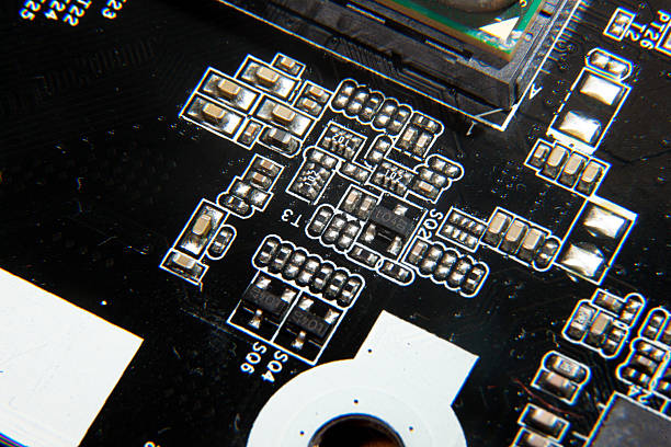
In the PCB production process, the Solder Mask Process is a critical step that directly affects product reliability, safety, and long-term performance. Its main objectives are achieving accurate alignment and creating a durable insulation layer.
Precise alignment ensures that the solder mask only covers non-soldering areas without blocking pads or circuit traces, providing sufficient space for subsequent soldering operations. Meanwhile, a uniform and dense insulation layer protects circuits from environmental exposure, preventing current leakage, short circuits, and oxidation.
As PCBs continue to develop toward higher density, miniaturization, and more complex designs, solder mask technology faces increasingly demanding requirements. Even minor alignment errors can cover solder pads and affect assembly quality, while insulation defects may lead to electronic failures or safety risks.
For manufacturers requiring reliable electronic solutions, professional PCB Manufacturing capabilities and strict process control are essential to achieving stable solder mask performance and high-quality circuit production.
1. Key Challenges Affecting Solder Mask Alignment and Insulation Performance
1.1 Major Challenges in Achieving Precise Alignment
The accuracy of solder mask alignment depends on the coordination between manufacturing processes, equipment precision, and operational control. Any small deviation during production can result in alignment failures.
One major challenge is substrate deformation. During earlier PCB manufacturing stages, such as copper deposition and etching, the board may experience slight expansion, contraction, bending, or stretching due to temperature changes and mechanical stress. If these deformations are not corrected before solder mask application, the actual positions of pads and traces may differ from the machine reference points, causing coating misalignment.
Equipment positioning stability is another important factor. During solder mask processing, machines typically rely on optical recognition systems or mechanical positioning methods to identify PCB locations. Contaminated camera lenses, optical path deviations, or worn positioning components may cause inaccurate recognition and result in incorrect solder mask coverage.
In addition, improper handling during production can also affect alignment accuracy. Small placement angles, uneven fixing pressure, or inconsistent operation procedures may create positioning deviations that impact later assembly processes.
For applications requiring precise and reliable assembly, professional SMT PCB Assembly technology helps ensure accurate component placement and compatibility with advanced PCB designs.
1.2 Potential Risks Affecting Insulation Performance
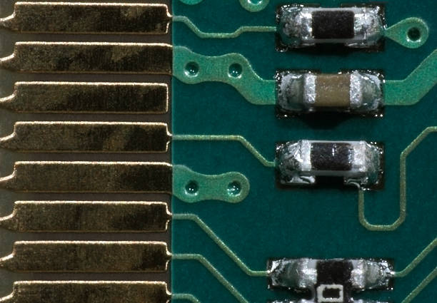
The insulation performance of solder mask layers depends on coating uniformity, material density, and adhesion strength. Poor process control can lead to several defects.
The first common issue is uneven coating thickness. If the coating equipment output speed fluctuates or PCB transportation speed is unstable, some areas may receive excessive coating while others remain too thin. Excessively thick areas may crack during curing, while thin areas may fail to provide sufficient electrical isolation.
The second risk involves air bubbles and impurities inside the solder mask layer. If solder mask materials absorb moisture during storage or are not properly mixed before application, trapped air and particles may form bubbles or pinholes after curing. These defects can become leakage paths and potentially cause short circuits.
The third issue is insufficient adhesion between the solder mask and PCB substrate. Surface contamination, oxidation, or incorrect curing temperatures may cause peeling or lifting of the solder mask layer, exposing circuits and reducing insulation reliability.
2. Practical Methods to Improve Solder Mask Alignment and Insulation Performance
2.1 Optimizing Substrate Preparation to Build a Strong Foundation
Substrate preparation is the foundation for achieving high-quality solder mask results. The main goals are eliminating deformation and ensuring surface cleanliness.
To control substrate deformation, manufacturers can introduce correction procedures before solder mask processing. Specialized leveling equipment can restore PCB flatness and ensure that pads and traces match standard positioning references.
During storage and transportation, dedicated supports should be used to prevent excessive stacking pressure and secondary deformation.
Surface cleaning is equally important. A complete cleaning process typically includes:
- Degreasing to remove oil contamination
- Micro-etching to eliminate oxidation and surface impurities
- High-pressure washing and hot-air drying to remove residues
After cleaning, PCBs should immediately enter the solder mask process to avoid secondary contamination and ensure strong adhesion between the coating layer and substrate.
2.2 Upgrading Equipment and Processes to Improve Alignment Accuracy
Precise solder mask alignment requires advanced equipment and strict process management.
Manufacturers should use solder mask coating equipment equipped with high-precision positioning systems. Dual-camera optical alignment technology is widely applied because it can identify reference points from multiple directions and automatically correct positioning errors.
Regular equipment calibration is also necessary. Cleaning optical components, checking positioning accuracy, and maintaining mechanical systems help ensure stable alignment performance.
From a process perspective, standardized positioning procedures should be established. Reference marks are placed on PCB surfaces, allowing automated systems to recognize board positions and define accurate coating boundaries.
During coating operations, closed-loop control systems can monitor PCB movement speed and automatically adjust material output to maintain consistent coating accuracy.
For different PCB sizes and structures, manufacturers should conduct small-batch verification before mass production to confirm alignment performance and reduce large-scale defects.
2.3 Controlling Solder Mask Materials and Curing Processes to Ensure Insulation
The insulation performance of solder mask layers is closely related to material quality and curing conditions.
Material management should begin with strict supplier evaluation. Important characteristics such as viscosity, drying speed, and insulation strength should be carefully tested before production.
During storage, solder mask materials must be kept in sealed conditions with controlled temperature and humidity to prevent moisture absorption or material degradation.
Before coating, materials should be thoroughly mixed to ensure uniform composition and prevent bubbles or particles from entering the coating layer.
The curing process also requires precise control. Manufacturers should optimize curing temperature curves based on material characteristics. A staged curing method is often preferred:
- Low-temperature pre-baking removes volatile substances
- Higher-temperature curing completes material hardening
This approach reduces the risk of cracking and bubble formation caused by sudden temperature increases.
After curing, controlled cooling procedures should be applied to prevent thermal stress and solder mask shrinkage.
For projects requiring complete production support, Turnkey PCB Assembly services can integrate manufacturing, material management, assembly, testing, and supply chain coordination to improve overall production efficiency.
2.4 Establishing Complete Quality Inspection Systems
A comprehensive inspection system is essential for maintaining solder mask quality throughout production.
For alignment inspection, high-resolution optical inspection equipment can scan completed PCBs and compare actual solder mask coverage with design specifications. If alignment deviations exceed acceptable limits, production parameters should be adjusted immediately and defective boards should be removed.
For insulation performance testing, manufacturers can use:
- Insulation resistance testing to detect leakage paths
- Voltage withstand testing to evaluate insulation stability
- Adhesion testing to verify bonding strength between solder mask and substrate
These tests help identify hidden defects that may affect product reliability.
A complete traceability system should also be established. Production parameters, material information, and inspection results for each PCB batch should be recorded. When quality problems occur, manufacturers can quickly identify root causes and implement corrective improvements.
3. Future Development Trends of Solder Mask Technology
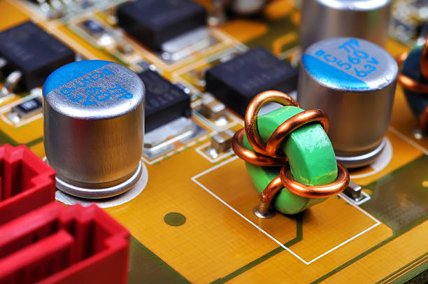
The ability to achieve precise alignment and excellent insulation performance depends on the combination of advanced materials, accurate equipment, optimized processes, and strict quality management.
As PCB designs continue moving toward higher density, smaller sizes, and more complex structures, solder mask technology must continue evolving.
Future improvements will focus on:
- Higher-resolution alignment systems
- More advanced solder mask materials
- Automated inspection technologies
- Intelligent manufacturing processes
For companies developing new electronic products, reliable partners with strong PCB Prototype Assembly capabilities can help validate designs quickly and optimize manufacturing performance before large-scale production.
Conclusion
Solder mask technology plays a fundamental role in ensuring PCB reliability and electrical safety. Achieving excellent alignment accuracy and insulation performance requires comprehensive control over substrate preparation, equipment precision, material quality, curing processes, and inspection systems.
By continuously improving manufacturing technologies and adopting advanced production methods, PCB suppliers can meet the growing demand for high-density and high-performance electronic products.
Professional PCB Manufacturing and assembly solutions enable companies to achieve higher product reliability, improved production efficiency, and stronger competitiveness in the global electronics market.