How to Achieve ±0.2mil Trace Width and Spacing Control in PCB Manufacturing
In advanced electronics manufacturing, trace width and spacing accuracy directly determine circuit density, signal integrity, and product reliability. The ability to achieve ±0.2mil precision has become one of the most important indicators of high-end PCB manufacturing capability.
This ultra-fine control standard requires not only advanced production equipment but also comprehensive management of materials, manufacturing processes, environmental conditions, and quality inspection systems.
With the rapid growth of miniaturized and highly integrated electronic products, achieving stable Trace Width and Spacing Control has become a key challenge for manufacturers seeking to overcome production limitations and ensure consistent product performance.
For companies developing advanced electronic products, professional PCB Manufacturing capabilities are essential to maintain precision, reliability, and production consistency throughout the entire manufacturing process.
1. Key Challenges Affecting ±0.2mil Trace Width and Spacing Accuracy
1.1 Material Characteristics Causing Precision Variations
The physical and chemical properties of materials are among the most important factors affecting trace width and spacing accuracy.
During PCB processing, substrates such as flexible materials and ceramic substrates may experience thermal expansion and contraction caused by temperature changes. Even minor deformation can stretch or shrink formed circuits, causing deviations beyond the ±0.2mil tolerance range.
For example, certain polymer materials may experience measurable dimensional changes during exposure and curing processes. When combined with errors from subsequent manufacturing stages, maintaining ultra-high precision becomes significantly more challenging.
Functional materials such as photoresist and conductive materials also influence final accuracy. Uneven photoresist viscosity can result in inconsistent coating thickness, affecting circuit edge definition after exposure. Meanwhile, conductive materials with inconsistent particle size may create rough circuit edges after printing, reducing trace uniformity.
Selecting stable materials and maintaining strict material control are essential foundations for achieving high-precision production.
1.2 Accumulated Errors During Manufacturing Processes
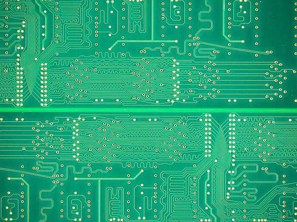
Ultra-fine trace width and spacing control involves multiple interconnected manufacturing stages. Small deviations in each process step can accumulate and eventually exceed acceptable limits.
During photolithography, exposure light stability and optical system cleanliness directly affect circuit resolution. Variations in light intensity can cause uneven photoresist exposure, resulting in traces that are too wide or too narrow.
Contaminants inside the optical path may also create shadows on the substrate surface, leading to dimensional errors.
During etching, parameters such as chemical concentration, temperature, and spray pressure must be precisely controlled. Excessive etching can reduce trace width, while insufficient etching may leave unwanted copper residues.
In addition, printing parameters such as scraper pressure and printing speed must be optimized. Incorrect settings can cause uneven conductive material transfer and create significant variations in circuit dimensions.
For applications requiring high accuracy from design to production, professional PCB Design Layout services help optimize circuit structures and improve manufacturability before production begins.
1.3 Hidden Environmental Factors Affecting Precision
Environmental conditions are often overlooked but can significantly influence ±0.2mil precision control.
Temperature fluctuations may cause thermal expansion in equipment structures, affecting positioning accuracy. Excessive humidity can cause photoresist materials to absorb moisture, changing their sensitivity and affecting exposure results.
Airborne dust particles are another potential risk. Contaminants attached to substrates or manufacturing tools may create defects such as missing traces or unwanted bumps.
Even mechanical vibration can affect ultra-precision equipment. External vibration sources may reduce positioning accuracy and create trace width and spacing deviations.
Therefore, maintaining a stable production environment is critical for consistent high-precision PCB manufacturing.
2. Practical Strategies for Achieving ±0.2mil Trace Width and Spacing Control
2.1 Material Management: Establishing a Reliable Precision Foundation
To minimize material-related variations, manufacturers must implement comprehensive material control systems.
During material selection, substrates with low thermal expansion coefficients and high dimensional stability should be prioritized. Ceramic substrates and specially modified polymer materials can help reduce deformation caused by temperature changes.
For functional materials such as photoresist and conductive pastes, strict incoming inspection is required. Important parameters include:
- Photoresist viscosity consistency
- Photosensitivity performance
- Coating uniformity
- Conductive material particle size
- Material flow characteristics
Storage conditions must also be controlled carefully. Temperature and humidity should remain within specified ranges to prevent moisture absorption, degradation, or performance changes.
A first-in-first-out inventory system helps ensure materials maintain their expected properties during production.
2.2 Process Optimization: Controlling Errors Across Every Stage
Optimizing manufacturing processes is one of the most effective ways to achieve ±0.2mil precision.
In photolithography processes, advanced exposure equipment with highly stable light sources and optimized optical systems improves circuit resolution.
Preheating substrates before exposure can also reduce thermal expansion and contraction effects during processing.
During etching, closed-loop control systems continuously monitor chemical concentration and temperature. When parameters move outside the required range, automatic adjustments can maintain stable etching performance.
Optimizing spray angles and pressure distribution ensures uniform chemical contact with circuit sidewalls, reducing uneven etching problems.
For manufacturers requiring flexible production solutions, Low-Volume PCB Assembly services provide reliable support for prototype validation and small-batch production while maintaining strict quality standards.
2.3 Equipment Upgrades: Improving Precision Control Capability
Production equipment determines the upper limit of trace width and spacing accuracy.
For positioning systems, high-precision linear motors combined with optical encoder feedback technology can significantly improve movement accuracy.
Linear motors provide fast and precise motion control, while encoder systems continuously monitor positioning errors and enable real-time corrections.
Advanced inspection equipment is equally important. Technologies such as laser measurement systems and high-resolution optical inspection systems can monitor trace dimensions during production.
If deviations exceed acceptable limits, the system can immediately issue alerts and prevent large-scale production defects.
In addition, equipment structures should use high-rigidity materials to minimize vibration and mechanical deformation during operation.
2.4 Environmental Control: Creating a Stable Manufacturing Environment
A controlled manufacturing environment is essential for maintaining ultra-high precision.
Production facilities should implement strict temperature and humidity management systems. Temperature fluctuations should be minimized, while humidity should remain within an appropriate range to protect materials and equipment performance.
Cleanroom systems are also important because airborne particles can directly affect circuit formation quality.
To reduce vibration interference, precision manufacturing areas should be isolated from vibration sources. Equipment should be installed on vibration-reduction foundations to prevent external disturbances from affecting processing accuracy.
Different production areas, including material storage, manufacturing, and inspection zones, should be separated to maintain stable environmental conditions.
2.5 Quality Monitoring: Establishing Full Process Traceability
A complete quality monitoring system ensures that precision deviations are detected and corrected quickly.
Before production, substrates should undergo inspection to verify surface quality and cleanliness.
During manufacturing, online inspection technologies can monitor trace width and spacing after each critical process stage. Production data should be recorded and analyzed to identify potential issues.
After completion, advanced inspection equipment such as high-resolution microscopy systems can verify final product accuracy.
A complete quality database should record:
- Manufacturing parameters
- Inspection results
- Material information
- Process conditions
This traceability system enables manufacturers to quickly identify causes of defects and continuously improve production performance.
For customers requiring complete manufacturing and assembly support, High-Volume PCB Assembly solutions provide scalable production capabilities while maintaining strict quality control.
3. The Future of Ultra-Precision PCB Manufacturing
Achieving ±0.2mil trace width and spacing control is not the result of optimizing a single production step. It requires coordinated improvements in materials, processes, equipment, environmental management, and quality systems.
As electronic products continue moving toward smaller sizes, higher integration, and faster signal transmission, the demand for ultra-precision PCB technology will continue increasing.
Future developments will focus on:
- More advanced substrate materials
- Higher-resolution imaging technologies
- Intelligent manufacturing systems
- Automated inspection solutions
Manufacturers with strong precision capabilities will be better positioned to support industries such as automotive electronics, medical devices, telecommunications, aerospace, and industrial automation.
Conclusion
Stable ±0.2mil trace width and spacing control represents a major achievement in advanced PCB manufacturing. It requires a complete production strategy covering material selection, process optimization, equipment upgrades, environmental control, and quality monitoring.
By adopting precision manufacturing technologies and advanced production management systems, PCB suppliers can deliver higher reliability, improved electrical performance, and stronger competitiveness in the global electronics market.
Professional PCB Assembly and manufacturing solutions allow customers to transform complex circuit designs into reliable, high-performance electronic products.