



5G Base Station RF Unit PCB Selection Guide
The RF unit of a 5G base station carries signal transmission, reception, filtering, and power amplification. These boards face high-frequency signals, real power density, heat, and interference at the same time. Outdoor cabinets add temperature swings and humidity to the list. The PCB is the physical platform under every RF component, so it shapes signal integrity, thermal behavior, and long-term reliability. Choosing one well means treating material, copper, mask, stackup, and test as one system rather than separate line items.
A buyer should start from the operating frequency, the power budget, and the deployment environment. Those three inputs set the material class, the copper weight, and the thermal path. They also decide how much impedance control and testing the project needs. Skipping this step leads to boards that pass a bench check and fail in the field. The sections below explain each decision, the tradeoffs behind it, and what to verify before you release a purchase order.
High-Frequency Material Choices
Material selection drives RF loss more than any other single decision. Standard FR-4 is economical and works for many general-purpose boards. As frequency rises, dielectric constant and dissipation factor matter more, and loss becomes a design limit. Depending on the design frequency and signal path, a specialized high-frequency laminate or a hybrid stackup may be the better fit. The right answer depends on the band, the path length, and the loss budget you can accept.
Check dielectric constant consistency across the operating band, not just at one test frequency. A stable Dk keeps transmission-line impedance predictable from design to production. Low dissipation factor reduces attenuation, which matters most on long RF runs and in filter sections. Also review coefficient of thermal expansion, moisture absorption, and dimensional stability. Outdoor equipment sees wide temperature swings, and a laminate that moves or absorbs moisture can warp, delaminate, or shift impedance over time.
Hybrid stackups mix materials to control cost. You might use high-frequency laminate only on the RF layers and standard material elsewhere. This approach works well when the design team defines which layers carry critical RF traces. It fails when the split is vague and the fabricator guesses. Document the material per layer, the expected Dk and Df, and the allowed tolerance in the fabrication drawing. Clear documentation keeps design, fabrication, and test teams working from the same numbers.
Copper Thickness and Current
Copper thickness links current capacity, thermal spreading, impedance, and manufacturability. A 5G RF unit often holds sensitive signal traces and high-current power sections on the same board. These areas do not need the same copper weight. For RF routing, heavy copper can shift transmission-line geometry and tighten manufacturing tolerances. At high frequency, surface finish and conductor loss also enter the picture. For power amplifier and distribution areas, more copper improves current handling and helps spread heat.
The practical approach is to set copper by circuit function, not by one global number. Review the required current, the target impedance, trace width and spacing, and the thermal load together. Then confirm the fabricator can hold those features at the chosen weight. Copper-to-laminate adhesion deserves attention on boards that see repeated thermal cycling. Differences in expansion between copper and dielectric stress the interconnections over time, so adhesion quality affects field life as much as electrical performance.
Solder Mask and Surface Protection
Solder mask protects copper from oxidation, contamination, and accidental contact. In RF designs, its electrical properties can also affect controlled-impedance structures. When mask overlaps or sits close to an RF trace, its dielectric behavior may need to enter the simulation. Some designs specify mask openings or mask-free zones over critical traces to keep performance predictable. Discuss these choices with the fabricator early, because mask configuration affects tooling and inspection.
A suitable mask should offer good insulation, strong adhesion, thermal resistance, and moisture resistance. Coating thickness should be consistent across the panel, and surface quality should support fine-pitch assembly. Outdoor units face dust, humidity, and temperature cycling, so a durable mask protects copper features through the service life. Surface flatness also matters where the board carries fine-pitch ICs, RF modules, connectors, or filters. Consistent mask processing supports reliable soldering and reduces assembly defects.
Thermal Path and Stackup
RF power amplifiers generate real heat in a small area. If that heat stays near the component, junction and board temperatures rise, performance drops, and aging speeds up. Thermal vias move heat from component pads into internal copper and toward a spreading structure. Large copper planes spread heat over a wider area and can double as ground or power distribution. For demanding cases, materials or structures with better thermal conductivity may be worth the cost.
Copper weight and layer stackup also shape heat flow. Extra copper or well-placed internal planes improve spreading in the right areas. Each addition should be checked against impedance, weight, and cost. Mechanical integration matters just as much. Board thickness and outline must match the enclosure, heat sink, shielding, and connector positions. A board with excellent electrical data can still fail if it does not fit the mechanical design. Plan thermal management during layout, not after the board is released.
Impedance Control and Verification
Impedance control keeps RF energy moving predictably from source to load. Trace width, dielectric thickness, copper weight, material Dk, and layer registration all shift the result. Small stackup changes on a multilayer RF board can move impedance enough to matter. Controlled-impedance work therefore starts with a defined stackup agreed between design and fabrication. Target impedance, reference planes, and allowed tolerances should be written down before tooling begins.
Verification closes the loop. Coupon testing and time-domain measurements confirm that the built board matches the design. Ask how the fabricator measures impedance, which coupons it uses, and how it records results. For production, agree on sampling and reporting so drift is caught early. For prototype and engineering builds, rapid PCBA prototyping helps teams confirm design, placement, and soldering before volume commitment. Early samples reveal pad geometry and process behavior while changes are still cheap.
Assembly and Test Coverage
Fabrication is only part of the job. RF modules carry fine-pitch ICs, connectors, filters, power devices, and shielding that demand precise placement and reflow. A supplier that handles both fabrication and assembly reduces handoffs and coordination risk. SMT PCB assembly with controlled paste volume and reflow profiles protects joint quality on dense RF boards. For mixed volumes, turnkey PCB assembly can cover sourcing, build, and test under one schedule.
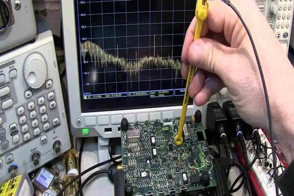
Test coverage should match the application. Electrical checks may include continuity, insulation resistance, dielectric withstand, and impedance. Functional test confirms the assembled unit works under power. Environmental checks such as temperature cycling, humidity, thermal shock, and vibration show whether the board holds up under stress. A structured PCBA testing plan ties these steps together and produces records you can review. Define the test requirements from the design and end-product specification, not from habit.
Supplier Checks Before Order
Price alone tells you little about a 5G RF supplier. Ask whether the factory can build your high-frequency or hybrid stackup, and whether it controls impedance consistently. Confirm it can handle your layer count, line and space, via structures, copper weight, and board size. Check support for thermal vias, heavy copper, and heat-spreader attachment. Ask what inspections and records come with each lot. A supplier that understands both RF performance and manufacturing limits will flag problems before they reach production.
Prototype support and production scalability matter too. You want engineering samples fast enough for design validation and a path to volume without a new supplier. Request process documentation, inspection data, and test reports for the first article. PCB assembly records should show which program ran, which materials were used, and what inspection found. Those records turn a field question into a fast answer and prove the fix reached the next batch.
Before you place the order, confirm the material suits the operating frequency and the Dk and Df limits are written down. Verify that controlled-impedance requirements are documented and that copper weight matches both RF and power needs. Check that thermal management is built into the stackup and that the mask suits the environment. Confirm board dimensions fit the mechanical assembly and that reliability and electrical tests are defined. Then confirm the supplier can actually build and test to those requirements.
The best board is the one matched to the real system, not the one with the most exotic material.