12-Layer PCB Manufacturing Challenges for Semiconductor Equipment
Semiconductor manufacturing equipment relies on highly complex electronic systems to control precision processes, transmit high-speed signals, manage power, and monitor critical operating parameters. In these systems, the PCB is not simply a platform for mounting components—it is an essential part of the electrical, thermal, and mechanical architecture.
A Semiconductor Equipment PCB may need to accommodate high-speed signals, power circuits, dense component placement, controlled impedance, thermal management, and demanding reliability requirements. When the board reaches 12 layers or more, manufacturing becomes significantly more challenging because every additional layer introduces more opportunities for dimensional variation, registration errors, warpage, and interconnection defects.
Compared with conventional multilayer boards, a 12-layer PCB requires tighter coordination between material selection, layer stack-up, lamination, drilling, plating, solder mask processing, inspection, and final quality control.
This article examines six major challenges in 12-Layer PCB manufacturing and explains what engineers and procurement teams should consider when selecting a manufacturing partner.
1. Multilayer Lamination: Maintaining Precise Layer Alignment
Lamination is one of the most critical stages in Multilayer PCB Manufacturing. A 12-layer board combines multiple copper layers, dielectric materials, prepregs, and cores into a single structure. Maintaining dimensional stability and layer-to-layer registration throughout this process is a major manufacturing challenge.
Layer Registration
Each circuit layer must be accurately aligned with the others. Even small registration deviations can affect:
- Via-to-pad alignment
- Trace geometry
- Controlled impedance
- Clearance between conductive features
- Signal integrity
- Component connectivity
During lamination, PCB materials are exposed to elevated temperature and pressure. Different materials can expand or contract at different rates, creating dimensional changes that must be carefully controlled.
As the number of layers increases, these dimensional changes become more difficult to manage. Proper stack-up engineering, material control, tooling strategies, and lamination parameters are therefore essential.
Overall Board Thickness
Thickness consistency is another important concern. Uneven pressure distribution or inconsistent resin flow can produce local thickness variations.
This can become especially problematic when the finished PCB must interface with precision connectors, mechanical assemblies, heat sinks, or other components with limited dimensional tolerance.
A qualified manufacturer should therefore control both overall board thickness and the dimensional stability of individual dielectric layers.
2. Microvia and Drilling Challenges
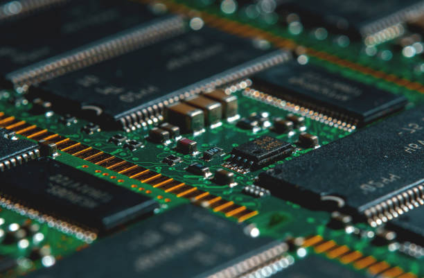
Complex semiconductor equipment often requires high-density interconnections to connect different signal and power layers. Depending on the design, through-holes, blind vias, buried vias, or microvias may be used.
For a high-density Semiconductor Equipment PCB, drilling and via fabrication require careful process control.
Drilling Accuracy
Small holes require accurate positioning and stable drilling conditions. Drill runout, tool wear, material characteristics, and board construction can all influence hole quality.
Poor drilling control may result in:
- Hole diameter variation
- Positional deviation
- Damaged hole walls
- Excessive burrs
- Inadequate copper plating
- Via reliability problems
Drill-tool management is therefore important for maintaining consistent hole quality throughout production.
Hole Wall Quality
After drilling, resin smear and debris may remain on the hole walls. Appropriate desmear and cleaning processes are necessary before copper plating.
If the hole wall is not properly prepared, the plated copper may not bond reliably to the surrounding material. Over time, thermal cycling and mechanical stress can then increase the risk of interconnection failure.
For high-reliability applications, via construction should be evaluated together with the PCB’s material system, aspect ratio, copper plating requirements, and reliability testing.
3. Copper Thickness: Balancing Uniformity and Local Current Capacity
Copper thickness can have a significant impact on electrical performance, thermal management, manufacturability, and reliability.
A 12-layer PCB used in semiconductor equipment may contain both sensitive signal-routing areas and power-distribution sections. These regions can have very different copper requirements.
Global Copper Uniformity
Copper plating must remain sufficiently consistent across the board to support predictable electrical and mechanical performance.
Plating distribution can be influenced by:
- Board geometry
- Pattern density
- Panel layout
- Plating current distribution
- Via structures
- Copper distribution between layers
Uneven copper deposition can affect conductor resistance, impedance characteristics, solderability, and thermal performance.
Localized Heavy Copper Requirements
Certain power or thermal areas may require more copper than standard signal-routing regions.
However, localized copper thickness creates additional manufacturing considerations. The transition between different copper structures can introduce surface-height differences and make solder mask application more difficult.
The PCB design should therefore consider copper distribution and manufacturability from the beginning rather than simply adding copper to high-current areas at a late design stage.
4. Solder Mask: Balancing Insulation, Coverage, and Precision
The solder mask protects exposed copper and helps prevent solder bridges and accidental electrical contact. For a 12-layer board used in semiconductor equipment, solder mask processing must provide consistent coverage while accommodating complex surface structures.
The challenge becomes greater when the PCB contains fine-pitch pads, dense routing, copper step differences, or specialized surface features.
Coating Uniformity
Solder mask thickness should be controlled consistently across the board. Insufficient coverage can reduce protection and insulation performance, while excessive or uneven coating may interfere with pads, connectors, or assembly processes.
The manufacturer must carefully control factors such as:
- Solder mask viscosity
- Coating or printing parameters
- Surface cleanliness
- Exposure conditions
- Developing process
- Curing conditions
Thermal and Chemical Resistance
Semiconductor equipment may operate in demanding environments, depending on its specific process and application. The solder mask should therefore be selected according to the expected temperature, humidity, chemical exposure, and service conditions.
Material selection and curing quality are particularly important for long-term reliability.
5. PCB Flatness and Warpage Control
Board flatness becomes increasingly important as PCB thickness, layer count, copper distribution, and structural complexity increase.
A 12-layer PCB can experience internal stresses during lamination and subsequent thermal processing. If these stresses are not properly balanced, the finished board may develop bow or twist.
Why Warpage Matters
Excessive PCB warpage can affect:
- Component assembly
- Connector engagement
- Mechanical installation
- Heat-sink contact
- Solder joint quality
- Automated assembly accuracy
Thermal management is particularly sensitive to flatness. If a high-power device or thermal interface does not make adequate contact with the intended heat-spreading structure, thermal resistance can increase.
Copper Balance
One effective design consideration is copper balancing.
If one region contains significantly more copper than another, thermal expansion and contraction may not occur uniformly. Maintaining a more balanced copper distribution across layers can help reduce manufacturing stress and improve dimensional stability.
This is why PCB layout should be evaluated not only from an electrical perspective but also from a manufacturing and mechanical standpoint.
For engineering teams developing complex multilayer boards, PCB Design Layout can help address layout and manufacturability considerations before fabrication.
6. Inspection and Quality Control for Complex Multilayer Boards
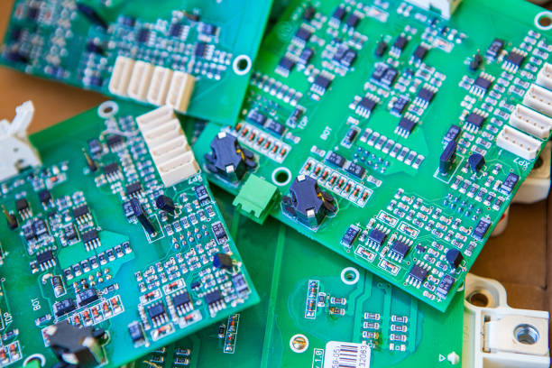
Inspection becomes increasingly important as PCB structure becomes more complicated.
Some defects on a 12-layer board may not be visible from the external surface. Internal layer defects, via problems, interlayer separation, or hidden connection issues require appropriate inspection methods.
Electrical Testing
Electrical testing can help identify:
- Open circuits
- Short circuits
- Incorrect connections
- Insulation problems
- Continuity issues
For controlled-impedance applications, impedance verification may also be required.
Automated Optical Inspection
AOI can detect many surface-level defects, including certain trace, pad, solder mask, and pattern abnormalities.
However, AOI cannot replace internal inspection for complex multilayer structures.
X-Ray Inspection
X-ray inspection can provide additional visibility into hidden structures such as vias and internal connections. It can be particularly useful when the PCB contains dense interconnections or complex structures.
The appropriate inspection strategy depends on the board design, manufacturing process, and customer quality requirements.
7. Why Process Control Is More Important Than Layer Count Alone
A common misconception is that the main difficulty of a 12-layer PCB is simply the number of layers.
In reality, manufacturing complexity is influenced by the combination of:
- Layer count
- Board thickness
- Material system
- Line width and spacing
- Via structure
- Aspect ratio
- Copper thickness
- Impedance requirements
- Surface finish
- Dimensional tolerances
- Thermal requirements
A relatively simple 12-layer board may be easier to manufacture than a lower-layer board with extremely fine features, demanding impedance specifications, unusual materials, or complex via structures.
For this reason, PCB manufacturers should evaluate the complete design rather than judging manufacturing difficulty solely by layer count.
8. Design-for-Manufacturing Considerations for 12-Layer PCBs
Early collaboration between the PCB designer and manufacturer can significantly reduce production risks.
Before releasing a 12-layer design for fabrication, engineers should review:
Stack-Up
Confirm the dielectric thickness, copper thickness, reference planes, and material properties.
Impedance
Define controlled-impedance requirements for high-speed signal paths and ensure the stack-up supports the target values.
Via Structure
Determine whether through, blind, buried, or microvia structures are actually necessary for the design.
Copper Distribution
Review copper balance across layers to minimize warpage and improve manufacturing stability.
Thermal Design
Identify high-power components and provide appropriate thermal paths through copper planes, thermal vias, or other structures.
Manufacturing Tolerances
Confirm that the specified line width, spacing, hole diameter, registration, board thickness, and other tolerances are achievable with the selected manufacturing process.
Early DFM review can prevent expensive redesigns and reduce the likelihood of manufacturing delays.
9. Prototype Validation Before Volume Production
For semiconductor equipment manufacturers, validating the PCB before mass production can be especially valuable because design changes become more expensive after integration into the complete machine.
A prototype run allows engineering teams to verify:
- Electrical performance
- Signal integrity
- Mechanical fit
- Thermal behavior
- Component compatibility
- Assembly quality
- Manufacturing consistency
For early-stage validation, Prototype PCB Assembly provides a way to evaluate both the bare PCB and assembled board before committing to larger production quantities.
For projects that require flexible production volumes during equipment development, Low-Volume PCB Assembly can also support engineering builds and smaller production requirements.
10. How to Select a 12-Layer PCB Manufacturer
When sourcing a High-Reliability PCB for semiconductor equipment, procurement teams should evaluate more than the supplier’s quotation.
Consider the following factors:
- Multilayer manufacturing capability – Confirm experience with 12-layer and other complex multilayer structures.
- Material capability – Check whether the supplier can work with the required laminate systems.
- Drilling and via capability – Evaluate the manufacturer’s ability to produce the required hole structures and aspect ratios.
- Impedance control – Confirm that controlled-impedance requirements can be consistently achieved.
- Copper plating control – Review the supplier’s ability to maintain reliable and consistent copper thickness.
- Inspection capability – Determine whether AOI, electrical testing, X-ray, and other relevant inspection methods are available.
- Quality management – Evaluate process documentation, traceability, inspection procedures, and corrective-action capabilities.
- Prototype support – Make sure engineering samples can be produced efficiently for design verification.
- Production scalability – Confirm that the supplier can support the project as it transitions from prototypes to production.
A reliable manufacturing partner should be able to discuss potential risks before production begins rather than simply accepting the Gerber files and quoting a price.
11. 12-Layer PCB Manufacturing Checklist
Before placing an order, review the following:
- Layer stack-up has been reviewed for manufacturability.
- PCB material is suitable for the application’s electrical and thermal requirements.
- Controlled impedance requirements are clearly defined.
- Copper thickness is appropriate for signal and power circuits.
- Via structures and drilling requirements are achievable.
- Copper distribution has been reviewed for balance.
- PCB flatness and warpage requirements are defined.
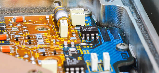
Printed Circuit Board - Solder mask specifications are appropriate for assembly and operating conditions.
- Surface finish has been selected according to component and assembly requirements.
- Electrical testing requirements are documented.
- Internal inspection requirements are defined where necessary.
- Prototype validation has been considered before volume production.
- The supplier has adequate quality-control and manufacturing capabilities.
Conclusion
Manufacturing a 12-layer PCB for semiconductor equipment is a complex engineering process that requires close control across every stage of production.
The major challenges include multilayer lamination, layer registration, microvia and drilling accuracy, copper thickness control, solder mask processing, PCB flatness, and internal quality inspection. These challenges become even more significant when the board must simultaneously support high-speed signals, power delivery, thermal management, and long-term reliability.
Successful manufacturing depends not only on advanced equipment but also on appropriate material selection, optimized stack-up design, controlled process parameters, effective inspection, and early DFM collaboration.
For semiconductor equipment manufacturers, selecting an experienced PCB Manufacturing partner can reduce production risks and provide a more reliable path from prototype validation to stable production. Gopcba supports PCB fabrication and assembly requirements for engineering development and production applications, helping customers manage complex PCB projects with greater manufacturing consistency.