How to Reduce Common Errors in PCB Prototyping: 5 Key Practices
PCB prototyping is a critical stage in electronic product development. It allows engineers to verify circuit functionality, validate the physical design, identify manufacturing problems, and prepare a product for future mass production.
However, prototype PCB projects can easily encounter problems when specifications are incomplete, materials are incorrectly selected, manufacturing processes are poorly coordinated, or quality checks are insufficient.
Many of these problems are not caused by highly complicated technologies. Instead, they often result from small mistakes made during preparation and production.
By focusing on five key areas, engineering teams and purchasing managers can significantly reduce the risk of prototype failures, unnecessary rework, material waste, and development delays.
1. Confirm Requirements Before Starting PCB Prototyping
Clear requirements are the foundation of successful PCB prototyping.
If important specifications are communicated only verbally or described in general terms, the manufacturer may have to make assumptions. Even a small misunderstanding at this stage can affect the entire prototype.
Important specifications may include:
- PCB dimensions
- Number of layers
- Board thickness
- Base material
- Copper thickness
- Surface finish
- Minimum trace width and spacing
- Hole and via requirements
- Impedance requirements
- Component density
- Assembly method
- Operating temperature
- Humidity and environmental conditions
- Electrical and functional testing requirements
For example, simply stating that a PCB must “withstand high temperatures” is not sufficient. The expected operating temperature, exposure duration, and relevant reliability requirements should be defined.
The same principle applies to surface finishes. If the PCB will be exposed to frequent connector insertion and removal, the selected finish should be evaluated according to the expected contact conditions and durability requirements.
A written specification checklist is therefore much more reliable than relying on informal communication.
For complex designs, working with a manufacturer that provides PCB Design & Layout support can also help identify potential design and manufacturing issues before fabrication begins.
2. Select and Verify Materials Carefully
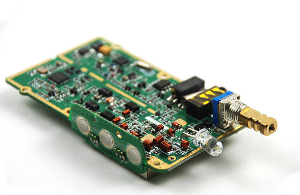
Material selection directly affects the electrical, thermal, mechanical, and manufacturing performance of a PCB.
One of the most common prototype errors is choosing a material without considering the actual application environment.
For example, a standard PCB material may not be suitable for an application with demanding thermal requirements. Similarly, copper thickness must be selected according to the electrical and current-carrying requirements of the circuit.
Common material-related issues include:
- Incorrect laminate grade
- Inappropriate board thickness
- Incorrect copper thickness
- Unsuitable surface finish
- Material incompatibility with the assembly process
- Incorrect auxiliary materials
- Expired or improperly stored materials
A reliable material verification process should include two stages.
Material Selection
The manufacturer should evaluate the material according to the PCB’s electrical, thermal, mechanical, and environmental requirements. The proposed material should then be confirmed before production.
Incoming Material Inspection
When materials arrive, their specifications should be checked against the purchase order and engineering documentation. Depending on the project, verification may include material grade, thickness, copper weight, certification, batch information, and other relevant parameters.
For high-risk applications, sample testing may be performed before committing to a larger quantity.
A capable PCB supplier should be able to explain how material selection affects the final PCB and recommend appropriate options rather than simply processing the files as submitted.
For advanced applications requiring specialized materials or structures, PCB Manufacturing capabilities covering multilayer, HDI, high-frequency, rigid-flex, and heavy-copper technologies can provide greater flexibility during prototype development.
3. Improve Coordination Across the Manufacturing Process
A PCB prototype involves multiple processes, and poor coordination between them can turn a minor problem into a major failure.
Depending on the project, production may involve:
- Material preparation
- Cutting
- Inner-layer fabrication
- Lamination
- Drilling
- Plating
- Imaging and etching
- Surface finishing
- Component assembly
- Soldering
- Inspection and testing
If an error occurs during one stage and is not identified before the next stage begins, additional work may be performed on an already defective board.
For example, if the PCB dimensions are incorrect but the problem is not detected after cutting, subsequent drilling and assembly operations may continue using the wrong dimensions. This can result in component-placement problems and unnecessary material waste.
To prevent this, manufacturers should establish clear process handoff procedures.
Each important production stage should record:
- Process completion status
- Inspection results
- Dimensional deviations
- Material abnormalities
- Surface defects
- Drilling problems
- Assembly issues
- Other manufacturing deviations
If an abnormality is discovered, production should be evaluated before the board proceeds to the next stage.
This becomes even more important when PCB fabrication and assembly are managed by different suppliers. A coordinated PCB Assembly process can simplify communication between fabrication, component procurement, SMT, through-hole assembly, inspection, and testing.
4. Implement Quality Inspection Throughout the Process
Quality inspection should not be limited to the final stage of prototype production.
If a manufacturing problem is discovered only after the entire prototype has been completed, correcting it may require significant additional time and cost.
A better strategy is to combine in-process inspection with final product testing.
In-Process Inspection
Inspection checkpoints can be established after critical operations.
For example:
- After cutting: verify board dimensions
- After drilling: inspect hole position and quality
- After plating: check surface and plating conditions
- After soldering: inspect solder joints
- Before final delivery: verify overall appearance and specifications
Final Testing
The completed prototype should be evaluated according to its intended application.
Testing may include:
- Electrical continuity
- Insulation resistance
- Contact resistance
- Functional testing
- Dimensional inspection
- Flatness
- Mechanical verification
- Signal performance
- Thermal testing
- Humidity testing
- Vibration testing
Not every PCB requires every test. The appropriate testing program should be based on the product’s operating environment, reliability requirements, and risk level.
For assembled prototypes, Prototype PCB Assembly provides a practical way to validate both the PCB and component assembly before moving toward larger production volumes.
5. Record Lessons Learned and Reuse Engineering Experience
Another effective way to reduce PCB prototype errors is to prevent the same problem from happening again.
If every prototype project is treated as an isolated job, valuable engineering experience can easily be lost.
For example, suppose a particular PCB repeatedly experiences soldering problems because of an unsuitable thermal profile. If the root cause is not documented, the same problem may occur on the next project.
Creating an engineering knowledge base or error database can help teams record:
- Error type
- Root cause
- Corrective action
- Material selection
- Manufacturing parameters
- Testing results
- Successful solutions
- Lessons learned
These records can then be referenced when developing similar PCB designs.
For example, previous experience with communication equipment, automotive electronics, industrial controls, or high-density boards can help engineers make better decisions when working on new projects.
Regular project reviews are also valuable. After completing a prototype, the engineering and manufacturing teams can evaluate what went well, what went wrong, and what should be changed in future production.
A Practical Checklist for Error-Free PCB Prototyping
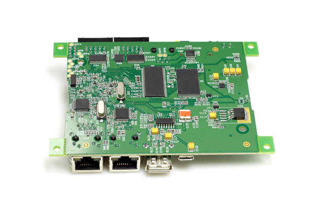
Before placing a prototype order, consider reviewing the following checklist:
- Confirm all PCB specifications in writing.
- Verify board dimensions and layer count.
- Confirm material type and copper thickness.
- Select the appropriate surface finish.
- Review design manufacturability.
- Confirm drilling and via requirements.
- Verify assembly requirements.
- Define inspection and testing requirements.
- Establish clear communication channels.
- Record design changes and engineering decisions.
- Review prototype results before mass production.
This approach helps transform PCB prototyping from a trial-and-error process into a controlled engineering validation process.
Why Choosing the Right PCB Supplier Matters
Reducing prototype errors is not solely the responsibility of the customer. The manufacturing partner also plays an important role.
An experienced PCB supplier should be able to identify obvious manufacturing risks, communicate potential problems, verify materials, coordinate production processes, and provide appropriate testing support.
For projects moving from prototype to small-batch production, a supplier that can support different production volumes can also reduce the risks associated with transferring the design between multiple manufacturers.
For example, Low Volume PCB Assembly can provide a practical transition between prototype validation and larger-scale production.
Conclusion
Common PCB prototyping errors are often caused by details that seem minor at the beginning of a project.
Unclear requirements can lead to incorrect manufacturing decisions. Poor material verification can compromise reliability. Weak process coordination can allow small problems to become major defects. Insufficient testing can leave critical issues undiscovered, while failing to document previous experience can cause the same mistakes to happen repeatedly.
The most effective solution is to build a prevention-oriented workflow covering requirements, materials, manufacturing, inspection, testing, and engineering feedback.
With clear documentation, careful material selection, coordinated manufacturing, comprehensive quality control, and continuous improvement, companies can reduce prototype failures, shorten development cycles, control costs, and create a smoother transition from prototype to mass production.