Common Multilayer PCB Lamination Problems and Effective Solutions
Lamination is one of the most critical processes in multilayer PCB manufacturing. By applying controlled heat and pressure, multiple inner layers and prepreg materials are bonded into a stable, reliable circuit board structure.
The quality of the lamination process directly affects the mechanical strength, insulation performance, dimensional stability, and electrical reliability of the finished PCB. If lamination defects occur, they can result in board rejection, additional processing costs, assembly problems, and even reliability issues in the final electronic product.
Because lamination performance is influenced by material properties, temperature, pressure, heating and cooling rates, equipment condition, and operating procedures, manufacturers need systematic process control rather than relying only on final inspection.
This article examines four common multilayer PCB lamination problems and explains practical ways to prevent and resolve them.
1. What Is the Main Goal of PCB Lamination?
The primary objective of PCB lamination is to achieve a strong, uniform bond between all layers while maintaining accurate alignment and dimensional stability.
During lamination, resin within the prepreg must soften and flow sufficiently to fill the spaces between copper layers and dielectric materials. At the same time, trapped air and volatile substances need to be effectively removed.
After curing and cooling, the multilayer structure should remain flat and firmly bonded without:
- Air bubbles or voids
- Delamination
- Excessive warpage
- Layer misalignment
- Resin starvation
- Excessive resin flow
These defects may have different appearances, but many originate from inadequate material preparation, improper process parameters, equipment variation, or inconsistent operator procedures.
For manufacturers handling complex multilayer boards, a controlled production process is therefore essential. Learn more about professional PCB Manufacturing capabilities and multilayer production technologies.
2. Four Common Multilayer PCB Lamination Problems
2.1 Air Bubbles and Voids Between Layers
What Does the Problem Look Like?
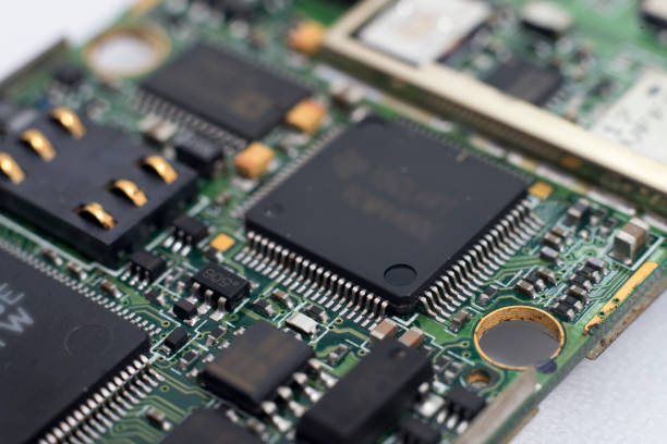
Small air bubbles or voids may appear inside the laminated structure or near the board surface. Some defects may remain hidden until subsequent drilling, soldering, or reliability testing.
Severe voids can reduce interlayer bonding strength and compromise insulation reliability.
Common Causes
Several factors can contribute to air bubbles during lamination:
- Moisture in prepreg: Improper storage can allow prepreg to absorb moisture. When heated, the moisture can vaporize and create internal voids.
- Contamination: Oil, dust, oxidation, or other contaminants on inner-layer surfaces can prevent proper resin bonding.
- Excessive heating rate: If resin melts and flows before trapped air has sufficient time to escape, air can become enclosed between layers.
- Insufficient resin: Inadequate resin content may prevent the material from completely filling gaps within the multilayer stack-up.
Recommended Solutions
Proper material preparation should begin before lamination. Prepreg should be stored under controlled conditions and dried according to the applicable material requirements when necessary.
Inner-layer surfaces should also be cleaned carefully before stacking. The surfaces must be dry and free from oil, dust, and other contaminants.
From a process perspective, the heating profile should be optimized so that resin has enough time to soften and flow while allowing trapped air to escape. Pressure should also be applied in coordination with the temperature profile rather than increasing too aggressively at the beginning.
Material inspection is equally important. Resin content, flow characteristics, shelf life, and storage conditions should be verified before production.
2.2 Delamination Between Layers
What Does the Problem Look Like?
Delamination occurs when bonded PCB layers separate or lose sufficient adhesion. It may become visible after mechanical stress, drilling, soldering, thermal cycling, or other subsequent processes.
In serious cases, the separation can significantly reduce mechanical strength and compromise long-term reliability.
Common Causes
Typical causes include:
- Incomplete resin curing
- Insufficient lamination temperature
- Inadequate curing time
- Insufficient bonding pressure
- Unsuitable inner-layer surface condition
- Oxidation or contamination on copper surfaces
If the resin does not reach the required degree of cure, the bond between layers may remain weak.
Recommended Solutions
The lamination temperature and curing time should be established according to the specific prepreg system rather than using a generic profile for every board.
Pressure must also be sufficient to ensure close contact between the layers and allow resin to properly wet the bonding surfaces.
Inner-layer surface treatment is another important consideration. The surface should provide suitable adhesion characteristics without excessive oxidation or contamination.
For certain applications, an additional post-cure process may be considered to further improve resin curing and interlayer bonding.
Strong PCB quality control should combine material verification, process monitoring, and physical reliability testing rather than depending entirely on visual inspection.
2.3 PCB Warpage and Deformation
What Does the Problem Look Like?
After lamination and cooling, a multilayer board may develop bow or twist instead of remaining flat.
Excessive warpage can create difficulties during PCB assembly. Boards may not sit correctly in fixtures, which can affect component placement, soldering, connector alignment, or mechanical installation.
Common Causes
One major cause is the difference in thermal expansion behavior between different materials.
During heating and cooling, copper, laminate, prepreg, and other materials expand and contract at different rates. If the structure is not properly balanced, internal stresses can accumulate and cause deformation.
Other possible causes include:
- Uneven cooling
- Excessively rapid cooling
- Uneven pressure distribution
- Unbalanced copper distribution
- Asymmetrical layer structures
- Inappropriate material combinations
Recommended Solutions
Material selection and stack-up design should be considered together. Using materials with compatible thermal expansion characteristics can help reduce internal stress.
The multilayer stack-up should also be balanced whenever possible. Copper distribution, dielectric thickness, and layer construction can all influence mechanical stability.
Cooling is another critical stage. Instead of rapidly reducing the temperature, a controlled cooling profile can give the laminated structure more time to release internal stress.
The lamination press should also be regularly maintained and calibrated to ensure uniform pressure and temperature distribution.
For complex boards, experienced engineers should evaluate the stack-up before production. This is particularly important for high-layer-count, thin, HDI, and high-density designs.
2.4 Layer Misalignment
What Does the Problem Look Like?
Layer misalignment occurs when inner-layer circuit patterns shift from their intended positions during the lamination process.
If the deviation becomes excessive, drilled holes may no longer align correctly with pads or inner-layer features. This can result in unreliable electrical connections or, in severe cases, unintended shorts between adjacent layers.
Common Causes
Common causes include:
- Damaged or unclear registration marks
- Incorrect inner-layer positioning
- Manual stacking errors
- Uneven lamination pressure
- Uneven thermal expansion
- Improper heating profiles
- Equipment-related alignment variation
Even a small alignment error can become significant when working with fine-pitch, high-density multilayer designs.
Recommended Solutions
Registration features should be clearly defined and inspected before stacking. Any damaged or unclear reference marks should be addressed before the lamination process begins.
Automated stacking and alignment systems can improve repeatability compared with purely manual operations.
The heating profile should also be controlled carefully to minimize uneven expansion. At the same time, press pressure should remain uniform across the working area.
After lamination, X-ray or other suitable inspection methods can be used to verify internal layer alignment. If a deviation is detected, engineering teams should determine whether it remains within the allowable tolerance before continuing with subsequent processing.
For advanced projects, precise alignment management is particularly important when manufacturing PCB Assembly products that require reliable connections between dense multilayer structures and components.
3. Preventive Process Control Is More Effective Than Corrective Action
Solving defects after they occur is important, but preventing them from occurring in the first place is much more efficient.
A reliable PCB manufacturing process should establish preventive controls throughout the entire lamination workflow.
Material Management
Prepreg and laminate materials should be stored according to manufacturer requirements. Storage conditions, shelf life, resin characteristics, and material specifications should be verified before use.
Critical materials should receive additional inspection when required, especially for demanding multilayer applications.
Standardized Lamination Parameters
Different board constructions require different lamination profiles.
Manufacturers should establish controlled parameters for:
- Temperature
- Pressure
- Heating rate
- Holding time
- Cooling rate
- Resin flow
- Vacuum conditions when applicable
Press temperature sensors, pressure gauges, and other monitoring equipment should be calibrated regularly.
Environmental Control
The production environment can also affect material performance.
Temperature and humidity should be controlled according to the materials and process requirements. Dust and contamination should be minimized, particularly in areas where inner-layer surfaces are prepared for lamination.
Operator Training
Even highly automated production lines depend on proper human operation.
Operators should understand material handling requirements, stacking procedures, registration methods, equipment settings, and defect-response procedures.
Clear work instructions and process checklists can reduce variation between production batches.
4. Why Lamination Quality Matters for Multilayer PCB Reliability
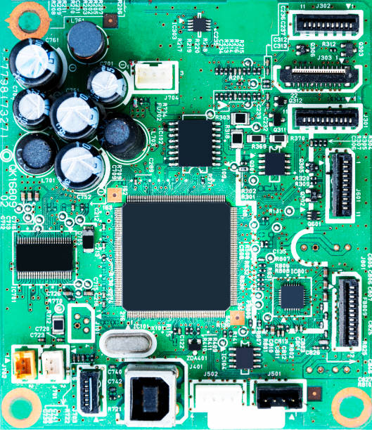
A multilayer board is not simply a collection of individual copper layers. Its long-term reliability depends on how effectively those layers are integrated into a mechanically and electrically stable structure.
Poor lamination can create problems that are not immediately visible. A board may pass a basic electrical test but later experience delamination, dimensional instability, insulation degradation, or other failures during thermal cycling and actual operation.
For this reason, prototype projects should also pay attention to lamination quality. A well-controlled Prototype PCB Assembly process can help engineers identify design, material, and manufacturing issues before moving into larger production volumes.
For customers developing new products, early validation can reduce the risk of repeating the same manufacturing problems during mass production.
5. Building a Reliable Lamination Quality Management System
A mature multilayer PCB supplier should manage lamination as part of an integrated quality system rather than treating it as an isolated manufacturing step.
A practical quality management framework should include:
- Material verification before production
- Stack-up and design review before fabrication
- Controlled lamination recipes for different board constructions
- Equipment calibration and preventive maintenance
- In-process inspection during critical manufacturing stages
- Internal alignment verification after lamination
- Electrical and physical testing before shipment
- Defect analysis and corrective action when abnormalities occur
- Production records and traceability for continuous improvement
This approach allows manufacturers to identify the root cause of defects rather than simply repairing or rejecting defective boards.
Conclusion
Multilayer PCB lamination is a precision manufacturing process that directly influences board strength, insulation performance, dimensional stability, and electrical reliability.
Air bubbles, delamination, warpage, and layer misalignment are among the most common lamination problems. Their causes can involve material moisture, surface contamination, inappropriate temperature and pressure profiles, uneven cooling, inaccurate stacking, or insufficient process control.
The most effective strategy is not simply to correct defects after they appear. Instead, manufacturers should establish preventive controls covering material management, stack-up design, lamination parameters, equipment calibration, environmental conditions, operator procedures, and inspection.
As multilayer PCBs continue to become thinner, denser, and more complex, lamination requirements will become increasingly demanding. Working with an experienced PCB supplier that understands material behavior, stack-up engineering, process control, and quality verification can help electronics manufacturers achieve more consistent results from prototype through production.
For projects that require controlled multilayer PCB fabrication and assembly, Low Volume PCB Assembly can also provide a practical path for validating manufacturing performance before scaling to higher production volumes.