How Are PCBs Manufactured? The Full Production Flow
A bare board starts as copper-clad laminate and leaves as a tested circuit. Between those points sit imaging, etching, lamination, drilling, plating, masking and inspection. Each step changes the panel in ways the next step cannot undo. That is why the flow matters more than any single machine. This guide walks the production sequence in order and explains what each stage decides.
The same discipline applies to PCB design and layout, where a small process drift turns into a large yield loss. A two-layer board follows a short path. Multilayer, HDI, high-frequency and rigid-flex boards add stages and tighten tolerances. The intent of every stage is the same: convert design data into a physical board that matches the drawing and survives assembly. Buyers who know the sequence ask better questions and spot weak quotes early.
Material Selection and Panel Cutting
Production begins with laminate choice. The material must meet the electrical, thermal and mechanical needs of the design. FR-4 covers most work, while high-frequency and high-temperature laminates serve demanding cases. The laminate arrives as a dielectric sheet with copper foil bonded to one or both faces. Engineers confirm the copper weight and dielectric thickness before release, because these values set impedance and current capacity.
The sheet is then cut into production panels sized for the board and the tooling rails. Panel size affects registration, drilling and routing later, so cutting accuracy matters. A small dimensional error at this point can shift every feature that follows. Many shops add coupon areas for test and cross-section work. Buyers should confirm that the panel layout leaves room for those coupons without eating into the board count.
Storage before cutting deserves a check of its own. Laminate absorbs moisture, and a damp panel can blister or measurably shift dimensions during lamination and reflow. Shops bake panels before pressing when the material calls for it, and they track humidity in the store. Buyers placing repeat orders should ask whether incoming laminate is checked for thickness and copper weight, and whether the certificate travels with the lot. A material substitution made quietly at this stage is hard to detect later.
Inner-Layer Imaging and Etching
For multilayer boards, inner layers are made first. A photosensitive dry film is laminated onto the copper. The film acts as a temporary mask that decides which copper survives etching. Surface preparation before lamination is critical, because contamination weakens adhesion and creates defects. The panel is then exposed through artwork, and the film hardens in the areas that must remain protected.
Development removes the unexposed film and reveals the copper to be etched away. Etching then strips that copper, leaving traces and pads. Over-etching narrows conductors, and under-etching leaves shorts. Both change electrical behavior, so line width and spacing are checked against the design. Automated optical inspection compares the finished pattern with reference data and flags opens, shorts, missing copper and pattern deviations. Catching these defects now keeps them out of lamination.
Registration is the quiet risk on inner layers. Each layer is imaged against tooling targets, and a small offset at this point becomes a misaligned via stack later. Shops measure the offset after etching and compare it with the allowed window. Buyers should ask how registration is verified and what happens when a layer drifts outside the limit. Scrap at this stage is cheap compared with a finished multilayer panel that fails electrical test.
Bond Treatment and Lamination
Before stacking, inner-layer copper receives a brown oxide or similar treatment. This roughens the surface and improves adhesion to the prepreg. The layers are then stacked with prepreg according to the approved stack-up and pressed under heat and pressure. The resin softens, flows and fills gaps between traces, then cures into a solid insulating structure. The result is one bonded multilayer panel.
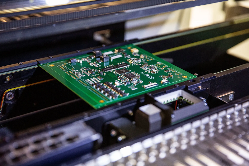
Temperature, pressure and heating rate all need control. Poor control produces delamination, voids, resin starvation and layer misregistration. These faults may pass visual checks and still fail in the field. Buyers should ask for the press cycle records and the stack-up drawing that was actually built. Any change in prepreg type or layer count means the lamination recipe must be reviewed again before the next run.
Resin flow is the variable that ties the press recipe together. Too little flow leaves voids around dense copper, and too much starves the bond at panel edges. The press profile is therefore matched to the copper distribution on each design, not copied from a similar board. Buyers with heavy copper or large plane areas should confirm that the shop reviewed the stack-up for fill and flow. A lamination fault often surfaces only at cross-section or thermal stress.
Drilling and Hole Preparation
Once laminated, the panel is drilled to the manufacturing data. Holes serve through-hole components, plated vias, mechanical mounting and tooling alignment. CNC drilling handles most mechanical holes, while laser drilling may form microvias in advanced HDI designs. Accuracy is critical because each hole must align with pads and internal copper across every layer. Drill wander or a worn bit can break that alignment.
Drilling leaves resin smear on hole walls where the bit passes through dielectric. This residue blocks electrical connection, so a desmear step removes it and prepares the wall for plating. Depending on construction, chemical or plasma methods may be used. The goal is a clean, uniform wall that accepts copper. Inspectors check hole size, position and wall quality before the panel moves to metallization.
Drill bit life is a practical control point that buyers rarely see. A worn bit cuts a rougher wall and raises the risk of smear and pad damage. Shops track hit counts per bit and change them on a schedule rather than on failure. Panel stack height and entry material also affect hole quality on thick boards. When a design has many small holes, ask how bit wear is managed, because the answer shows up in via reliability.
Plating and Outer-Layer Circuits
Hole walls are non-conductive after drilling. Electroless copper deposits a thin conductive layer over the walls and surfaces. Electrolytic plating then builds copper to the required thickness. The barrel must connect every layer it passes through, so plating uniformity is checked rather than assumed. Thin or voided plating creates vias that fail under thermal cycling.
Outer layers are then imaged and plated to form the final circuit. The sequence includes film lamination, exposure, development, pattern plating, a protective tin layer, stripping, etching and inspection. The aim is to keep designed copper and remove the rest. Fine traces and tight spacing demand precise control here. A second optical inspection confirms the outer pattern before solder mask goes on. Buyers reviewing PCB assembly plans should confirm the board data matches the assembly drawing at this point.
Current distribution decides plating thickness across the panel. Features near the plating contacts usually build faster than features at the far edge, so shops use thieves and shielding to even the field. Buyers ordering boards with high aspect ratio holes should ask how surface and hole copper are measured. A coupon cross-section gives the answer in numbers. Plating that looks fine on the surface can still hide a thin barrel that cracks in service.
Solder Mask and Silkscreen
Solder mask covers most copper and protects it from oxidation, solder bridging and handling damage. It is applied across the panel, then exposed and developed to open pads and other soldering areas. After curing, the mask becomes a durable layer. Inspection looks for incomplete coverage, misalignment, scratches and blocked openings. A mask opening that is too small can cause poor joints during SMT PCB assembly.

Silkscreen prints reference designators, polarity marks, connector labels and test-point identifiers. Placement must stay clear of pads and soldering areas, or the ink interferes with the joint. The ink is cured for adhesion and durability. Buyers should check that the silkscreen revision matches the assembly files, because a stale reference can send a technician to the wrong part during rework or repair.
Surface Finish and Electrical Test
Exposed copper pads need a finish that protects the metal and accepts solder. ENIG gives a flat surface for fine-pitch parts. HASL is widely used and cost-effective. Immersion tin and immersion silver suit specific assembly needs, and OSP protects copper while keeping a solderable surface. Hard gold or edge plating serves contact fingers that face wear. The choice depends on assembly method, storage life, contact use and budget.
Electrical testing then verifies connectivity. Continuity and isolation checks detect opens and shorts, and net verification confirms the board matches the design data. Complex boards with many nets need full test coverage, not sampling. Test programs should be tied to the same data used to build the board. Teams planning PCBA testing later should agree on test access now, because missing test points limit what can be checked.
Finish selection also sets the storage clock. OSP and immersion silver are sensitive to handling and time, while ENIG and HASL tolerate longer storage. Buyers should match the finish to the assembly date, not just to the solder process. A board that sits for months before build can oxidize and cause wetting faults. Ask for the finish date and the recommended shelf life, and plan the build window around them.
Routing, Final Inspection and Cost
The panel is separated into boards by routing, milling, punching or scoring. The outline must match the mechanical drawing, including slots, cutouts, V-grooves and edge connectors. Dimensional checks confirm board size and hole position. Final inspection then combines visual review, AOI, electrical test and, where needed, cross-section analysis. Records from these checks should travel with the lot, because they answer questions months later.
Cost follows complexity. Layer count, board size, material, copper weight, hole count, via types, finish and quantity all move the price. Tighter traces and special processes add steps and inspection time. Reviewing the design for manufacturability before release usually cuts cost without touching performance. Buyers comparing quotes should ask what is included, since a low figure often hides test coverage or finish choices. A partner offering turnkey PCB assembly can align fabrication and assembly checks under one data set.
A controlled flow links every stage to the next. Material choice sets dimensional stability. Inner-layer registration sets multilayer connectivity. Drilling and plating decide via reliability. Mask and finish decide assembly yield. None of these can be fixed by final inspection alone. The practical takeaway for buyers is simple: request the stack-up, the inspection records and the test report with each order, then compare suppliers on those documents rather than on the headline price.