In modern Multilayer PCB design, mechanical features such as slots, cutouts, and non-circular plated or non-plated holes are increasingly common. These features are widely used for connector interfaces, mechanical positioning, heat dissipation, component clearance, and structural requirements.
Unlike conventional round drilled holes, PCB Slots and obround pads require additional manufacturing information to clearly define their dimensions, locations, and connections. If the design data is incomplete or ambiguous, the PCB manufacturer may interpret the feature incorrectly, potentially resulting in manufacturing defects or even tool damage.
This article explains practical methods for defining slots and obround pads in PCB Design, including mechanical-layer definitions, overlapping pads or vias, NC drill data, internal-plane connections, and manufacturing data verification.
1. Why PCB Slots and Obround Pads Require Special Attention
A conventional circular hole can generally be described using a drill diameter and coordinate. A slot, however, has both a width and a length, and its shape and orientation must be clearly communicated to the manufacturer.
An obround pad also requires more information than a standard circular pad. The pad geometry, hole dimensions, copper area, layer span, and electrical connection must all be correctly defined.
For a Multilayer PCB, the situation becomes more complicated because a slot may cross several copper layers, dielectric layers, or internal planes.
Therefore, the design data should clearly communicate:
- Slot length and width
- Slot location and orientation
- Plated or non-plated status
- Start and end layers
- Pad geometry
- Internal-layer clearance
- Electrical connection requirements
- Manufacturing and drilling information
The goal is to ensure that the PCB designer and manufacturer interpret the same mechanical feature in exactly the same way.
2. Common Methods for Defining PCB Slots
Depending on the PCB CAD software and the manufacturer’s CAM process, there are several methods for defining PCB Slots.
The three commonly used approaches include:
- Defining detailed slot information on a mechanical layer
- Using overlapping pads or vias to represent the slot geometry
- Generating dedicated NC drill or routed-slot manufacturing data
Among these methods, using a dedicated mechanical layer to describe slot information is often easier for manufacturers to interpret, provided that the layer definition has been agreed upon in advance.
However, the exact data format should always be confirmed with the PCB Manufacturing supplier before production.
3. Defining Slot Information on a Mechanical Layer
For many PCB designs, the mechanical layer is used to communicate the location and geometry of a slot.
The mechanical drawing should clearly identify:
- Slot outline
- Slot centerline
- Slot length
- Slot width
- Start and end points
- Plated or non-plated requirements
- Relevant component reference designators
- Additional manufacturing notes
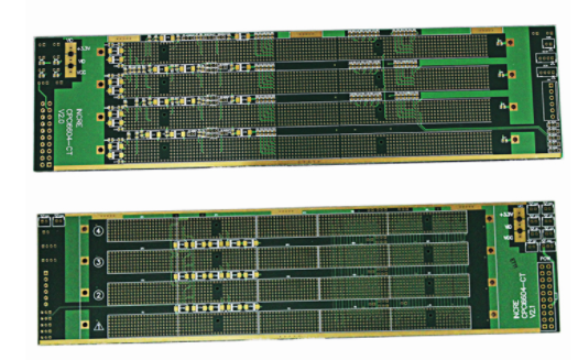
For example, a connector may require several elongated mounting slots. The mechanical layer can provide the manufacturer with the exact dimensions and locations required for these features.
When the design is viewed in single-layer mode, the slot definition and associated copper features can be inspected independently. This is useful for verifying whether the mechanical information corresponds correctly with the copper layers and component footprints.
Designers should also confirm that the selected mechanical layer is included in the final manufacturing output. A slot definition that exists only inside the CAD environment but is not transferred to the manufacturing package can easily be missed during fabrication.
4. Using Pads or Vias to Define Slot Geometry
Another approach is to use multiple overlapping pads or vias to describe the required slot area.
In some CAD environments, two pads positioned at the opposite ends of a slot can be combined with a defined connection between them to represent an elongated hole.
However, this method must be used carefully.
If overlapping pads, vias, or drill objects are interpreted incorrectly by the CAM system, the resulting drill data may contain duplicated or conflicting instructions. In extreme cases, the manufacturing equipment could attempt to process the same location incorrectly.
Therefore, overlapping pads or vias should not be used simply because they visually resemble a slot. The method must be compatible with the manufacturer’s CAM and drilling workflow.
Before adopting this approach for production, the designer should provide the data to the PCB manufacturer and confirm that the intended slot can be correctly interpreted.
5. Using NC Drill and Routed-Slot Data
A more manufacturing-oriented approach is to generate dedicated NC Drill or routed-slot information.
Unlike a simple drawing representation, NC manufacturing data can provide the machine or CAM system with explicit information about the required mechanical operation.
Depending on the manufacturing process, a slot may be produced by:
- CNC routing
- Slot drilling
- Specialized drilling tools
- Combination routing and drilling processes
The appropriate method depends on the slot dimensions, material structure, tolerance requirements, plating requirements, and the manufacturer’s equipment capability.
For complex Multilayer PCB designs, the designer should not assume that every slot can be manufactured using the same drilling method as a conventional plated through-hole.
6. Defining Slot Dimensions Correctly
When defining a slot, the designer should provide sufficient information for the manufacturing engineer to determine the final machined geometry.
For example, the design should specify:
- Overall slot length
- Slot width
- Centerline
- Start and end coordinates
- Corner radius where applicable
- Plating requirement
- Layer range
For an obround slot, the width is normally related to the cutting tool or finished slot diameter, while the overall length defines the final mechanical opening.
The distinction between tool-path length and finished slot length should also be clarified when necessary. Different CAM systems may interpret the geometry differently depending on whether the supplied data represents the finished profile or the cutter centerline.
7. Internal Plane Connections Around Slot Pads
One of the most important considerations in Multilayer PCB design is the connection between obround pads and internal power or ground planes.
A slot pad may not connect to an internal plane in the same way as a conventional circular pad. The designer therefore needs to check the plane clearance and thermal connection around the entire pad geometry.
For example, if a connector pad is connected to an internal power plane, sufficient copper clearance must be provided around the slot and its associated pad structure.
Depending on the design requirements, the connection may use:
- Direct plane connection
- Thermal relief connection
- Custom copper geometry
- Dedicated copper regions around the slot
The appropriate approach depends on current requirements, thermal performance, manufacturability, and the PCB manufacturer’s process capability.
8. Managing Plane Connections for Obround Pads
For obround pads connected to power or ground planes, the CAD design rules should be configured carefully.
A dedicated pad class or design-rule configuration can be used to control how these pads connect to internal planes. This is especially useful when only certain slot pads require a different connection style from standard pads.
Designers should verify:
- Whether the pad is connected to the intended plane.
- Whether the plane clearance is sufficient.
- Whether the thermal relief geometry is manufacturable.
- Whether the connection meets the required current capacity.
- Whether the plane connection is correctly represented in the output data.
The final result should always be checked in the actual layer stack rather than relying only on the CAD editor’s visual appearance.
9. Special Considerations for Negative Internal Planes
Internal power and ground planes in a Multilayer PCB may use negative-image or negative-plane data.
This can create additional challenges when a slot pad is expected to connect to an internal plane.
In some cases, the slot area may appear visually correct in the PCB design software but fail to create the intended electrical connection in the final manufacturing output.
If the CAD system does not automatically generate the required connection, designers may need to define additional copper geometry or modify the plane connection settings.
Any additional copper object should be added deliberately and verified against the intended electrical net. It should not be used as an arbitrary graphical object.
10. Verification Before Manufacturing Output
Before releasing the design for PCB Manufacturing, designers should perform a complete manufacturing-data review.
Special attention should be given to:
- Slot dimensions
- Slot locations
- Slot orientation
- Plated/non-plated requirements
- Pad geometry
- Drill sizes
- Internal-plane connections
- Copper clearances
- Mechanical-layer information
- NC drill output
- Gerber output
- ODB++ or other manufacturing databases
If the latest CAD/CAM tools provide manufacturing-data inspection capabilities, designers should use them to verify the actual output files rather than checking only the original PCB layout.
This distinction is important because the design database and the exported manufacturing files are not necessarily identical representations.
11. Gerber and ODB++ Output Considerations
When exporting Gerber Files, the mechanical layer containing slot information should be included if it is part of the agreed manufacturing documentation.
For ODB++ or other intelligent manufacturing formats, the designer should verify that the slot geometry, layer information, pad definitions, and relevant attributes are correctly transferred.
The manufacturing package should clearly communicate whether the slot is:
- Plated
- Non-plated
- Routed
- Drilled
- Part of a component footprint
- Connected to a copper plane
Ambiguous manufacturing data can lead to unnecessary engineering clarification, production delays, or incorrect fabrication.
12. Communicating With the PCB Manufacturer
A reliable PCB Manufacturing process depends not only on correct CAD design but also on clear communication between the designer and manufacturer.
Before using a special slot-definition method, designers should confirm with the manufacturer:
- Which mechanical layers are accepted for slot definitions
- Whether routed slots are supported
- How plated slots should be specified
- How non-plated slots should be specified
- Whether overlapping pads or vias are acceptable
- Which NC drill format is required
- How minimum slot width is controlled
- What dimensional tolerance can be achieved
At Kingda, designers can work with the manufacturing engineering team to confirm the appropriate data structure for special mechanical features before production.
This approach helps reduce ambiguity and ensures that the design intent is correctly transferred from the CAD environment to the manufacturing process.
13. Practical Design Checklist
Before releasing a PCB containing slots or obround pads, use the following checklist:
- Confirm the slot dimensions.
- Confirm the slot location and orientation.
- Specify plated or non-plated requirements.
- Verify the start and end layers.
- Check the pad and hole geometry.
- Check internal-plane clearances.
- Verify thermal or direct plane connections.
- Confirm the mechanical layer is included in the manufacturing package.
- Review NC drill and routing data.
- Inspect the final Gerber or ODB++ output.
- Confirm the manufacturing method with the PCB supplier.
These steps are particularly important for high-density and complex Multilayer PCB designs, where mechanical and electrical requirements often overlap.
Conclusion
Creating PCB Slots and Obround Pads requires more than simply drawing an elongated hole in a PCB layout. The designer must consider mechanical dimensions, manufacturing methods, pad geometry, internal-plane connections, drilling or routing data, and final manufacturing-output verification.
Mechanical-layer definitions, overlapping pads or vias, and dedicated NC Drill or routing data can all be used to communicate slot information, but the most appropriate method depends on the CAD system and the manufacturer’s CAM process.
For reliable PCB Design and PCB Manufacturing, the key is to ensure that every special mechanical feature has an unambiguous definition and can be correctly interpreted by the manufacturer. By reviewing the manufacturing data before release and confirming special requirements with Kingda, designers can reduce fabrication risks and improve the consistency of the final PCB.