How to Determine PCB Layer Count: PCB Layers, Stackup & Inspection Guide
The rapid development of electronics and automation has made the PCB (Printed Circuit Board) an essential part of almost every modern electronic product. From consumer electronics and industrial automation equipment to automotive systems, telecommunications, medical devices, and aerospace applications, increasingly sophisticated functions are being integrated into smaller and more compact products.
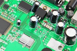
As circuit complexity increases, routing all signals on a single or double-sided board can become impractical. This challenge led to the widespread adoption of the multilayer PCB, in which multiple conductive layers are separated by dielectric materials and laminated into a single board structure.
Knowing the PCB layer count is important when designing, manufacturing, repairing, inspecting, or reverse engineering a circuit board. However, determining the number of layers is not always as simple as counting the visible copper patterns on the top and bottom surfaces. Internal signal layers, power planes, ground planes, blind vias, buried vias, and microvias may all be hidden inside the board.
For this reason, engineers use a combination of design documentation, visual inspection, electrical analysis, cross-sectional examination, X-ray inspection, and other advanced techniques to determine how many layers a PCB has.
This guide explains the structure of PCB layers and provides practical methods for accurately determining PCB layer count.
What Are PCB Layers?
A PCB layer is a conductive or structural layer within a printed circuit board stackup.
In a simple board, copper may exist only on one side. In a multilayer design, several copper layers are separated by dielectric insulating materials and bonded together during the lamination process.
Depending on the design, PCB layers may serve different purposes, including:
- Signal routing
- Power distribution
- Ground reference
- High-speed signal routing
- RF signal routing
- Thermal management
- Electromagnetic shielding
A typical multilayer PCB may contain a combination of:
- Outer copper layers
- Inner signal layers
- Ground planes
- Power planes
- Prepreg dielectric layers
- Core dielectric layers
- Solder mask
- Surface finishes
It is important to distinguish copper layers from the total number of physical layers in a PCB. Solder mask and silkscreen are surface-processing layers, but they are not normally counted as conductive PCB layers.
Common PCB Layer Configurations
PCB designs may be classified as:
| PCB Type | Typical Structure | Common Applications |
|---|---|---|
| Single-sided PCB | One copper layer | Simple electronics, low-cost products |
| Double-sided PCB | Two copper layers | Industrial controls, consumer electronics |
| 4-layer PCB | Four copper layers | Embedded systems, networking, power electronics |
| 6-layer PCB | Six copper layers | High-density digital and industrial systems |
| 8+ layer PCB | Multiple signal/plane layers | High-speed, computing, telecom, complex electronics |
| HDI multilayer PCB | Fine lines, microvias, sequential build-up | Compact, high-density electronics |
There is no universal maximum or minimum layer count for all PCB applications. The appropriate number depends on routing density, electrical requirements, mechanical constraints, manufacturing technology, cost, and reliability requirements.
More layers do not automatically mean better performance. The PCB stackup must be designed appropriately for the intended electrical and mechanical requirements.
Why Is PCB Layer Count Important?
Determining the PCB layer count is important for several reasons.
PCB Design
Layer count directly affects routing capacity and stackup design.
PCB Manufacturing
Manufacturers need accurate layer information to fabricate the correct core, prepreg, copper, drilling, and lamination structure.
PCB Repair
Technicians may need to know which signals or planes are located inside the board when troubleshooting damaged connections.
PCB Reverse Engineering
When the original design files are unavailable, determining the internal layer structure is an important part of reconstructing the PCB.
Signal Integrity Analysis
High-speed circuits depend on controlled relationships between signal traces and reference planes. Knowing the layer arrangement is therefore essential for analyzing impedance and return paths.
Thermal and Power Design
Power planes, copper distribution, thermal vias, and copper thickness all influence electrical and thermal behavior.
How to Determine PCB Layer Count
There is no single method that works for every board. The most appropriate approach depends on whether the original design documentation is available and how complex the PCB is.
The following methods range from the simplest non-destructive techniques to advanced inspection methods.
1. Check the PCB Design and Manufacturing Documentation
The most reliable method is to check the original design documentation.
If available, review:
- Native PCB design file
- PCB stackup drawing
- Fabrication drawing
- Gerber files
- Drill files
- Assembly documentation
- Manufacturer documentation
- Material specifications
- Engineering change records
A proper PCB stackup drawing can show the number and sequence of copper and dielectric layers directly.
For example, a simplified six-layer stackup could be:
L1 Signal → Dielectric → L2 Ground → Dielectric → L3 Signal → Dielectric → L4 Power → Dielectric → L5 Ground → Dielectric → L6 Signal
The actual arrangement varies according to the design.
Why Documentation Is the Best Starting Point
Documentation eliminates much of the guesswork involved in physical inspection.
However, it is important to understand that Gerber files are manufacturing artwork rather than a complete editable PCB design database. A complete manufacturing package normally contains multiple Gerber layers and separate drill data.
Therefore, simply opening one Gerber file does not tell you the complete PCB layer count. The complete fabrication data set must be reviewed.
2. Perform a Visual Inspection
Visual inspection is the simplest way to begin determining PCB layers.
Inspect both sides of the board for:
- Copper patterns
- Pads
- Vias
- Through-holes
- Component locations
- Ground areas
- Large copper regions
- Board-edge structure
- Silkscreen markings
A double-sided PCB normally has visible copper routing on both sides.
However, visual inspection alone cannot reliably determine the complete layer count of a multilayer PCB because internal copper layers are hidden.
Examine the PCB Edge
The edge of a PCB can sometimes provide useful information.
If the board edge is exposed and sufficiently clear, the different dielectric and copper structures may be visible.
A magnifying glass or microscope can make these features easier to inspect.
However, edge inspection is not always conclusive. Surface finishes, solder mask, board construction, edge treatments, and manufacturing tolerances can make individual layers difficult to distinguish.
Therefore, edge inspection should generally be treated as an initial estimation rather than definitive proof.
3. Analyze Through-Holes, Blind Vias, and Buried Vias
Via structures provide important clues about the PCB stackup.
Through Vias
A through via extends through the PCB and can connect multiple copper layers.
Its presence confirms that the board contains more than one conductive layer, but it does not by itself reveal the exact total layer count.
Blind Vias
A blind via connects an outer layer to one or more internal layers without passing completely through the PCB.
Blind vias can provide clues about the stackup and routing architecture.
Buried Vias
A buried via connects internal copper layers and does not normally reach an outer surface.
Because buried vias are hidden inside the board, they are more difficult to identify through ordinary visual inspection.
Microvias
Microvias are very small vias commonly used in HDI PCB construction.
They may connect adjacent layers in a sequential build-up structure.
The presence of microvias can indicate a sophisticated multilayer or HDI structure, but the exact layer count still requires additional evidence.
4. Use Electrical Tracing and Continuity Testing
Electrical analysis can provide additional information when documentation is unavailable.
A digital multimeter can be used to check electrical relationships between:
- Pads
- Vias
- Test points
- Connectors
- Component pins
- Ground locations
- Power locations
By mapping connections, engineers can gradually reconstruct portions of the circuit.
If a visible surface trace disappears into a via, it may continue on another layer.
However, continuity testing cannot directly tell you how many physical PCB layers exist.
It is primarily a method for understanding connectivity and supporting reverse engineering.
Important Measurement Consideration
A low resistance or continuity indication does not automatically prove that two points are directly connected by a PCB trace. Parallel circuit paths, low-resistance components, power planes, and other circuit elements can affect measurements.
Therefore, electrical measurements should be interpreted in the context of the circuit rather than used as the sole method for determining layer count.
5. Use PCB Design and Layout Software
If the original PCB design files are available, PCB design software provides one of the easiest ways to determine PCB layer count.
A native PCB design file can contain information about:
- Copper layers
- Signal layers
- Power planes
- Ground planes
- Vias
- Pads
- Component footprints
- Nets
- Routing
- Board outline
- Design rules
- Stackup configuration
Engineers can switch individual layers on and off to examine the board layer by layer.
This approach is particularly useful when reviewing complex multilayer PCB designs.
Gerber Files
Gerber files can also be reviewed to identify manufacturing artwork for individual copper layers.
For example, a fabrication package may contain artwork corresponding to:
- Top copper
- Inner copper 1
- Inner copper 2
- Inner copper 3
- Bottom copper
Together with other fabrication data, these files can provide strong evidence of the board’s conductive layer structure.
However, Gerber data should be interpreted as a manufacturing data set rather than as a complete original PCB design.
6. PCB Cross-Section Analysis
When accurate physical information is required, cross-section analysis is one of the most direct methods.
A small section of the PCB is removed, typically from an appropriate area that will not compromise the board’s required analysis objectives.
The exposed cross-section can then be:
- Mounted
- Ground and polished
- Etched when appropriate
- Examined under a microscope
- Documented through imaging and measurement
A cross-sectional image can reveal:
- Copper layers
- Dielectric layers
- Prepreg
- Core materials
- Plated through-holes
- Via structures
- Copper thickness
- Layer spacing
Optical microscopy is commonly sufficient for many cross-section analyses, while scanning electron microscopy (SEM) can provide higher-resolution information when required.
Advantages of Cross-Section Analysis
- Direct observation of internal construction
- High structural accuracy
- Useful for failure analysis
- Useful for manufacturing verification
- Suitable for detailed reverse engineering
Limitation
Cross-section analysis is destructive because part of the PCB is removed.
For an operational product, the sample selection should therefore be carefully planned.
7. X-Ray Inspection
X-ray inspection is a valuable non-destructive method for examining internal PCB structures.
Because X-rays can penetrate the board, they can reveal features that cannot be seen through ordinary visual inspection.
X-ray inspection may help identify:
- Internal vias
- Through-hole structures
- Hidden solder joints
- Large internal copper structures
- Component connections
- Some aspects of multilayer construction
Automated X-ray inspection (AXI) is widely used in electronics manufacturing, particularly for inspecting hidden solder joints and assembly defects.
However, standard 2D X-ray images may not always provide enough information to determine every layer unambiguously.
8. CT Scanning
Computed tomography (CT) scanning provides three-dimensional X-ray imaging.
Compared with conventional 2D X-ray inspection, CT can provide a more detailed representation of internal structures.
Depending on equipment resolution and PCB construction, CT analysis may reveal:
- Internal copper structures
- Via connections
- Layer relationships
- Component interconnections
- Internal defects
- Structural anomalies
CT is particularly useful for complex boards where non-destructive internal analysis is required.
However, resolution, board size, material composition, and feature density can affect the usefulness of CT results.
9. Use Advanced Microscopy and Imaging
For highly detailed analysis, engineers may combine:
- Optical microscopy
- Digital microscopy
- SEM
- X-ray imaging
- CT scanning
- Cross-sectional analysis
These methods can be selected according to the required level of accuracy.
For example, optical microscopy may be sufficient for routine PCB cross-section inspection, while SEM may be useful for examining very small structures or material interfaces.
How to Determine PCB Layer Count From a Physical Board
When the original documentation is unavailable, a practical workflow is:
Step 1: Inspect Both Sides
Determine whether copper routing exists on one or both outer surfaces.
Step 2: Inspect the Board Edge
Look for visible copper and dielectric structures.
Step 3: Examine Via Types
Identify through vias, blind vias, buried vias, and microvias where possible.
Step 4: Map Important Connections
Use a multimeter and other instruments to investigate major nets.
Step 5: Examine Available Manufacturing Data
If Gerber and drill files are available, analyze the complete fabrication package.
Step 6: Use X-Ray or CT
If internal construction remains uncertain, use non-destructive imaging.
Step 7: Perform Cross-Section Analysis
When the highest level of physical certainty is required, analyze a prepared PCB cross-section.
Step 8: Document the Stackup
Record:
- Layer number
- Layer function
- Copper thickness
- Dielectric thickness
- Via structures
- Material structure
The result should be compared against available design or manufacturing information whenever possible.
Challenges in Determining PCB Layer Count
Determining the PCB layer count can become difficult for several reasons.
HDI PCB Structures
HDI PCBs may contain microvias, sequential build-up layers, fine lines, and complex via structures.
These features make the internal structure much more difficult to infer from external appearance.
Blind and Buried Vias
Blind and buried vias can hide layer transitions and make manual tracing difficult.
Flexible and Rigid-Flex PCBs
Flexible PCBs and rigid-flex PCBs can have unusual layer structures and may not visually resemble conventional rigid multilayer boards.
Internal Copper Planes
Ground and power planes may occupy large internal areas without producing obvious surface routing.
Embedded Components
Some advanced PCB constructions can include embedded passive or other structures, making external inspection insufficient for complete analysis.
Damaged or Repaired Boards
Burned areas, corrosion, delamination, repair wires, reconstructed pads, and other modifications can obscure the original construction.
Best Practices for Determining PCB Layers
The following practices can improve accuracy when determining PCB layers.
Start With Existing Documentation
Always check the original stackup, fabrication drawing, native PCB design data, and manufacturing files before performing physical analysis.
Use Non-Destructive Methods First
Start with:
- Visual inspection
- Design-file analysis
- Gerber review
- Electrical measurements
- X-ray
- CT
Only use destructive cross-section analysis when necessary.
Do Not Rely on One Visual Clue
The number of visible traces, vias, or board-edge lines does not necessarily equal the total number of copper layers.
Combine multiple sources of evidence.
Record Every Observation
During reverse engineering, document:
- Component locations
- Via positions
- Net connections
- Layer assumptions
- Measurements
- Images
- Cross-section results
- Design revisions
This creates traceability and makes later verification easier.
Confirm Before Manufacturing
If a PCB is being reproduced, do not begin manufacturing based only on an estimated layer count.
The complete stackup, material system, copper thickness, drill structure, impedance requirements, and fabrication specifications should be established before production.
PCB Layer Count vs. PCB Stackup
These two concepts are related but not identical.
PCB layer count generally describes the number of conductive copper layers.
PCB stackup describes the complete vertical construction of the board, including:
- Copper layers
- Core materials
- Prepreg
- Dielectric thickness
- Solder mask
- Surface finishes
- Other structural materials
For example, a four-layer PCB does not simply consist of four copper sheets. It also contains dielectric materials between the conductive layers.
A proper PCB stackup determines the physical relationship between signal layers and reference planes, which can strongly affect controlled impedance, signal integrity, capacitance, and electromagnetic behavior.
Why PCB Layer Count Matters for High-Speed Design
In high-speed electronics, layer count should not be considered independently from stackup design.
A well-designed multilayer PCB may use dedicated or strategically positioned reference planes to provide predictable return paths for high-speed signals.
Important factors include:
- Dielectric thickness
- Trace width
- Trace spacing
- Copper thickness
- Reference-plane location
- Via transitions
- Return-path continuity
- Impedance control
Simply adding more layers does not automatically improve signal integrity.
The complete stackup and routing strategy must be designed together.
PCB Layer Count and Manufacturing
Accurate layer information is essential for PCB manufacturing.
A multilayer PCB requires carefully controlled:
- Material selection
- Lamination
- Layer registration
- Drilling
- Plating
- Etching
- Impedance control
- Surface finishing
- Electrical testing
As layer count and structural complexity increase, manufacturing challenges can also increase.
For this reason, the PCB layer count should be established early in the engineering process rather than treated as a simple visual characteristic of the finished board.
How Kingda Supports Multilayer PCB Projects
Accurate layer information is essential when moving a design into PCB manufacturing.
Kingda can support multilayer PCB projects based on the required manufacturing documentation and specifications. Depending on the project, this may include:
- Gerber data
- Drill files
- PCB stackup requirements
- Board specifications
- Copper thickness requirements
- Controlled-impedance requirements
- Fabrication drawings
- Electrical testing requirements
For complex multilayer projects, customers should provide a consistent and complete manufacturing data package whenever possible.
If a physical board is being reproduced through reverse engineering, the layer count should be verified together with the stackup, materials, copper thickness, via structures, and other critical construction parameters.
Conclusion
Learning how to determine PCB layer count is an important skill for PCB design, manufacturing, maintenance, failure analysis, and reverse engineering.
The simplest boards may provide enough information through documentation and visual inspection. However, modern multilayer PCB designs can contain hidden signal layers, power planes, ground planes, blind vias, buried vias, and microvias that cannot be accurately identified from the board surface alone.
The most reliable approach is to use a progressive inspection strategy:
Documentation → Visual Inspection → Via Analysis → Electrical Testing → PCB Data Analysis → X-Ray/CT → Cross-Section Analysis
Whenever possible, start with the original PCB stackup and manufacturing documentation. If these are unavailable, combine multiple inspection techniques rather than relying on a single visual clue.
For advanced or high-density boards, X-ray and CT inspection can provide valuable non-destructive information, while cross-section analysis offers direct evidence of the physical layer structure when destructive analysis is acceptable.
Ultimately, determining the PCB layer count is only one part of understanding a multilayer board. A complete analysis should also consider the PCB stackup, material system, copper thickness, dielectric structure, via technology, routing architecture, and electrical requirements.
By combining accurate documentation with systematic inspection and engineering analysis, manufacturers and engineers can obtain a much clearer understanding of complex PCB structures and make better decisions during design, repair, reverse engineering, and production.