Custom PCB Design and Manufacturing: Custom PCB Board Process, Benefits & Applications
As electronic products become smaller, smarter, and more multifunctional, conventional printed circuit boards (PCBs) are often no longer sufficient to meet increasingly complex system requirements. A standard PCB is typically designed around a defined circuit architecture and a specific set of electrical, mechanical, and environmental requirements. While this approach works well for many applications, advanced products may require multiple circuit functions, specialized interfaces, compact packaging, and application-specific performance within a single system.
This is where Custom PCB technology becomes increasingly important.
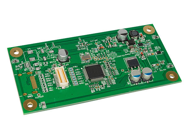
A Custom PCB Board can integrate multiple functional circuits, interfaces, power-management sections, control circuits, communication modules, and other electronic functions into a purpose-built design. Instead of using several independent boards for different functions, engineers can integrate selected functions into one optimized PCB or develop interconnected subassemblies that work together as a complete system.
A well-designed Custom PCB can therefore help engineers address application-specific requirements such as size constraints, electrical performance, thermal management, component integration, connectivity, and manufacturing requirements.
This guide explains the key stages of Custom PCB Design, Custom PCB Manufacturing, assembly, testing, and how to choose an appropriate manufacturing partner.
What Is a Custom PCB?
A Custom PCB is a printed circuit board designed and manufactured specifically for a particular product, system, or application rather than being based solely on a standard board configuration.
Depending on the application, a custom board may include:
- Analog and digital circuits
- Microcontrollers (MCUs) or processors
- Power-management circuits
- RF and wireless communication interfaces
- Sensors and signal-conditioning circuits
- High-speed interfaces
- Connectors and cable interfaces
- Thermal-management structures
- Specialized mounting features
- Embedded or integrated functional modules
A custom design can be single-sided, double-sided, or multilayer. It may also use rigid, flexible, or rigid-flex construction depending on mechanical and electrical requirements.
For complex products, several smaller PCBs may also function as subassemblies within a larger electronic system. The important objective is not simply to combine as many functions as possible onto one board, but to create an architecture that balances electrical performance, manufacturability, reliability, cost, and product size.
Why Use a Custom PCB?
Modern electronic products are expected to provide more functionality while occupying less physical space. Using a separate PCB for every function can increase the total system size, wiring complexity, connector count, assembly effort, and potential failure points.
A properly engineered Custom PCB can provide several advantages.
Functional Integration
Multiple circuit functions can be integrated into one PCB or coordinated through purpose-built subassemblies. This can simplify system architecture and reduce unnecessary interconnections.
Space Optimization
PCB dimensions, component placement, connector locations, and layer stackup can be optimized around the available product enclosure.
This is particularly useful for compact consumer electronics, industrial equipment, medical devices, automotive electronics, and other space-constrained systems.
Application-Specific Electrical Performance
A custom design allows engineers to optimize parameters such as:
- Controlled impedance
- Signal integrity
- Power distribution
- Grounding and return paths
- Electromagnetic compatibility (EMC)
- Thermal performance
- High-current routing
- RF performance
These requirements are difficult to address effectively with a generic board.
Flexible Interfaces
Connectors, mounting holes, test points, communication interfaces, and other mechanical or electrical features can be positioned according to the final system requirements.
Potential System-Level Cost Reduction
Although a custom PCB may require additional engineering effort and initial tooling or development costs, integrating functions can reduce the number of separate boards, connectors, cables, and assembly operations. The overall economic benefit should therefore be evaluated at the system level rather than based solely on bare PCB cost.
Planning a Custom PCB
Successful Custom PCB Design begins long before PCB layout.
A standard PCB already requires careful consideration of electrical, mechanical, and manufacturing requirements. A custom design generally requires even closer coordination between product engineers, PCB designers, component engineers, assembly teams, and the PCB manufacturer.
Before starting the schematic, engineers should define the fundamental requirements of the project.
Key Questions to Define
Important questions include:
- What functions must the PCB perform?
- What are the maximum PCB dimensions?
- What enclosure or mechanical constraints apply?
- Is the board a complete product PCB or a subassembly?
- How will different circuit sections communicate?
- What power sources and voltage rails are required?
- What are the expected current levels?
- Are high-speed, RF, or sensitive analog signals involved?
- What components and connectors are required?
- What environmental conditions will the PCB encounter?
- What production volume is expected?
- What testing and regulatory requirements apply?
- What are the target cost and manufacturing schedule?
Answering these questions early helps establish a realistic design direction and reduces expensive redesigns later.
Custom PCB Layout Design
Once the functional requirements have been finalized, the PCB Layout Design process can begin.
The first step is normally to develop a complete schematic containing all required components, functional blocks, interfaces, and electrical connections.
1. Schematic Design and Simulation
The schematic should clearly define the electrical architecture of the PCB.
Depending on the project, engineers may use simulation and analysis tools to evaluate:
- Power behavior
- Analog performance
- Digital timing
- Signal integrity
- Component interactions
- Thermal behavior
- RF characteristics
- Potential design errors
Simulation cannot replace physical testing, but it can identify many design problems before PCB fabrication.
2. PCB Stackup Definition
For multilayer boards, the PCB stackup should be defined before detailed routing.
The stackup determines the arrangement of copper layers, dielectric materials, reference planes, and other structural elements. It directly affects:
- Controlled impedance
- Signal integrity
- Power distribution
- Electromagnetic compatibility
- Mechanical thickness
- Thermal behavior
- Manufacturability
Not every custom PCB requires a large number of layers. The appropriate layer count should be determined by routing density, electrical requirements, component technology, mechanical constraints, and manufacturing capability.
3. Component and Footprint Selection
Components should be selected based on electrical performance, availability, lifecycle, package type, environmental requirements, and manufacturing considerations.
Both SMD components and PTH components may be used depending on the application.
Engineers should also verify:
- Footprint dimensions
- Pin assignments
- Package orientation
- Polarity
- Component height
- Thermal requirements
- Keep-out areas
- Assembly accessibility
- Supply-chain availability
For custom products, component selection can have a major impact on both PCB performance and long-term production stability.
4. PCB Placement and Routing
Component placement should follow the functional architecture of the circuit.
Sensitive analog circuits, high-speed interfaces, power circuits, RF sections, and heat-generating components may need to be physically separated or carefully arranged to minimize unwanted interactions.
During routing, engineers should consider:
- Trace width
- Trace spacing
- Signal length
- Differential-pair routing
- Controlled impedance
- Reference planes
- Return-current paths
- Via placement
- Thermal vias
- Copper areas
- High-current paths
- EMI/EMC considerations
The goal is not simply to connect every net, but to create a PCB that is electrically sound, mechanically compatible, thermally manageable, and manufacturable.
5. Design Documentation
A complete PCB Design package should normally include the appropriate manufacturing and assembly information.
Depending on the project, documentation may include:
- Schematic files
- PCB layout files
- Gerber or Gerber X2 files
- NC drill files
- Bill of Materials (BOM)
- Pick-and-place data
- Assembly drawings
- Fabrication drawings
- Stackup information
- Impedance requirements
- Special manufacturing instructions
- Test requirements
A complete documentation package gives the manufacturer a reliable basis for fabrication and assembly.
Custom PCB Manufacturing Process
The Custom PCB Manufacturing process follows the design requirements established during engineering. Although the fundamental manufacturing technologies are similar to those used for standard PCBs, custom boards may require specialized materials, stackups, drilling structures, surface finishes, controlled impedance, unusual dimensions, or other application-specific processes.
1. Select the Right Custom PCB Manufacturer
Choosing an appropriate Custom PCB Manufacturer is one of the most important steps in the project.
Not every PCB manufacturer supports every combination of materials, layer counts, copper thicknesses, tolerances, HDI structures, surface finishes, or assembly requirements.
When evaluating a manufacturing partner, consider:
- Manufacturing capabilities
- Engineering support
- DFM/DFA review
- Material availability
- Layer-count capability
- Fine-line and fine-pitch capability
- HDI capability when required
- Surface-finish options
- PCB assembly capability
- Inspection and testing
- Production volume flexibility
- Quality-control processes
- Lead time
- Communication and technical support
For complex projects, early communication between the design team and manufacturer can prevent manufacturability problems before production begins.
2. Material and Component Selection
Material selection is particularly important for a custom board.
Depending on the application, engineers may select materials such as:
- FR-4
- High-Tg FR-4
- High-frequency laminates
- PTFE-based materials
- Polyimide
- Metal-core materials
- Ceramic substrates
- Flexible PCB materials
The material should be selected according to electrical, thermal, mechanical, environmental, and cost requirements.
Component selection should also consider product lifecycle and supply-chain risks. A technically suitable component may still create production problems if it is difficult to source or likely to become obsolete.
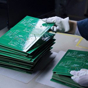
3. PCB Fabrication
The PCB fabrication process typically includes several major stages.
Material Preparation
The appropriate laminate and copper-clad material are prepared according to the specified board construction.
Inner-Layer Fabrication
For multilayer PCBs, inner copper layers are imaged, developed, etched, and inspected to create the required circuit patterns.
Lamination
Multiple circuit layers are combined with dielectric materials such as prepreg under controlled temperature and pressure.
Accurate registration during lamination is critical for multilayer and high-density designs.
Drilling
Mechanical drilling and, when required, laser drilling are used to create through-holes, microvias, blind vias, or other required structures.
Copper Plating
Plating processes create conductive connections between appropriate PCB layers and build the required copper thickness on hole walls and circuit features.
Outer-Layer Processing
The outer copper layers are patterned and processed to form the final external circuitry.
Solder Mask
A solder mask is applied to protect exposed copper areas and help prevent unintended solder bridging during assembly.
Surface Finish
A suitable surface finish, such as ENIG, HASL, OSP, or another specified finish, may be applied depending on the component, soldering process, storage requirements, and application.
Silkscreen
Silkscreen markings can identify reference designators, polarity indicators, labels, test points, and other assembly information.
Electrical and Dimensional Inspection
Finished boards may undergo electrical testing, automated optical inspection, dimensional inspection, and other quality checks according to the product requirements.
For complex Custom PCB Boards, manufacturing controls become especially important because small deviations in registration, drilling, plating, or etching can affect electrical performance and assembly yield.
Custom PCB Assembly Process
After PCB fabrication, the bare board can be assembled with the required components.
The PCB Assembly Process typically includes the following stages.
1. Solder Paste Printing
For SMT assembly, solder paste is deposited onto designated PCB pads using a stencil.
The stencil design, paste volume, alignment, and printing parameters must be controlled carefully, particularly for fine-pitch components.
2. SMT Component Placement
Automated pick-and-place equipment positions SMD components according to the PCB assembly data.
Component orientation, polarity, package type, placement accuracy, and feeder setup must be verified.
3. Reflow Soldering
The assembled PCB passes through a reflow oven where a controlled thermal profile melts the solder paste and forms solder joints.
The thermal profile should be compatible with the PCB materials, components, solder paste, and assembly requirements.
4. Through-Hole Assembly
If PTH components are required, they can be installed using manual insertion, automated insertion, wave soldering, selective soldering, or other suitable methods.
The correct assembly method depends on component geometry, board construction, production volume, and thermal requirements.
5. Inspection and Rework
After assembly, boards may undergo AOI, X-ray inspection, visual inspection, or other methods depending on component types and product requirements.
Any identified defects should be analyzed and corrected using controlled rework procedures.
Testing and Troubleshooting of Custom PCBs
Testing is a critical part of the Custom PCB Manufacturing process because a successful fabrication and assembly process does not automatically guarantee that the complete electronic system will function correctly.
Testing should be defined according to the product’s electrical and functional requirements.
Common PCB Testing Methods
Automated Optical Inspection (AOI)
AOI can identify many visible assembly defects, including:
- Missing components
- Incorrect component placement
- Polarity errors
- Solder bridges
- Insufficient solder
- Misalignment
X-Ray Inspection
X-ray inspection is useful for assemblies containing hidden solder joints, such as certain BGA packages and other bottom-terminated components.
In-Circuit Testing
ICT can evaluate selected electrical characteristics and detect certain manufacturing defects when appropriate test access and fixtures are available.
Functional Testing
Functional testing evaluates whether the assembled PCB performs its intended functions under defined operating conditions.
Depending on the product, testing may include:
- Power-up verification
- Communication testing
- Sensor testing
- Analog measurement
- Digital I/O testing
- RF testing
- Load testing
- Firmware verification
- System-level functional testing
Troubleshooting Custom PCB Problems
If a custom board fails testing, troubleshooting should follow a structured process.
Engineers may review:
- The original schematic
- PCB layout
- BOM
- Assembly data
- Manufacturing records
- Test results
- Component specifications
- Power rails
- Signal paths
- Mechanical and thermal conditions
Electrical measurements, oscilloscope analysis, thermal inspection, and other diagnostic methods may then be used to isolate the root cause.
How to Improve Custom PCB Manufacturing Reliability
A reliable custom board requires more than a good schematic. Design and manufacturing decisions should be coordinated from the beginning.
Apply DFM and DFA
Design for Manufacturing (DFM) helps ensure that the PCB can be fabricated consistently.
Design for Assembly (DFA) helps ensure that components can be placed and soldered efficiently.
Applying these principles before production can reduce manufacturing defects and unnecessary redesigns.
Consider Thermal Management Early
High-power components should be evaluated for heat generation and heat dissipation.
Possible solutions include:
- Large copper areas
- Thermal vias
- Heavier copper
- Appropriate PCB materials
- Heat sinks
- Metal-core construction
- Improved airflow
The appropriate approach depends on the actual thermal load and system architecture.
Plan for Testing
Test points, programming interfaces, fixture access, and diagnostic features should be incorporated into the design when appropriate.
A PCB that is easy to manufacture but difficult to test can create significant production and service challenges.
Manage Component Availability
A custom PCB can remain technically functional while becoming commercially difficult to manufacture if critical components become obsolete or unavailable.
Lifecycle management should therefore be considered during component selection.
Conduct Prototype Validation
Before mass production, prototypes or pilot builds can be used to verify:
- Electrical performance
- Mechanical fit
- Thermal behavior
- Assembly quality
- Signal integrity
- Firmware operation
- System functionality
Design changes are generally easier and less expensive to implement before production volume increases.
Custom PCB Applications
Custom PCB technology is used across many industries where standard board configurations cannot fully satisfy product requirements.
Common applications include:
- Consumer electronics
- Automotive electronics
- Industrial automation
- Medical equipment
- Telecommunications
- Networking equipment
- IoT devices
- Power electronics
- LED systems
- Security equipment
- Test and measurement equipment
- Aerospace and defense electronics
Each application may impose different requirements for materials, reliability, dimensions, electrical performance, environmental resistance, and testing.
Custom PCB vs. Standard PCB
| Feature | Standard PCB | Custom PCB |
|---|---|---|
| Design | Based on defined configurations | Application-specific |
| Dimensions | Often standardized or constrained | Optimized for the product |
| Circuit functions | Usually predefined | Designed around required functions |
| Components | Selected from standard requirements | Selected for application-specific needs |
| Layer stackup | Common configurations | Customized as required |
| Interfaces | Standardized | Application-specific |
| Thermal design | General requirements | Optimized for actual thermal load |
| Manufacturing | Established process | May require specialized processes |
| Development effort | Generally lower | Generally higher |
| Flexibility | Limited | High |
| Typical use | General-purpose products | Specialized or complex products |
It is important to note that “custom” does not necessarily mean “more layers” or “more complicated.” A custom PCB can be relatively simple if the application requires a unique shape, connector arrangement, mechanical interface, or circuit function.
How Kingda Can Support Custom PCB Projects
A successful Custom PCB Manufacturing project requires coordination between PCB design, fabrication, assembly, component sourcing, testing, and product requirements.
Kingda can support customers with custom PCB projects by helping align PCB specifications with manufacturing and assembly requirements. Early technical communication can help identify potential issues involving board dimensions, stackup, components, routing, manufacturability, assembly, and testing before production.
For complex products, this engineering-oriented approach can help reduce unnecessary redesigns and improve the transition from prototype development to production.
The exact manufacturing and assembly capabilities should always be evaluated against the requirements of the individual project.
Conclusion
As electronic products continue to integrate more functions into smaller form factors, Custom PCB Design and Custom PCB Manufacturing are becoming increasingly important.
A successful custom board is not simply a PCB with additional components. It is the result of coordinated planning across circuit architecture, component selection, PCB layout, stackup design, manufacturing, assembly, testing, thermal management, and product-level requirements.
From the initial schematic and PCB Layout Design to fabrication, PCB Assembly, inspection, and functional testing, every stage can influence the reliability and performance of the final product.
By defining requirements early, applying DFM/DFA principles, selecting appropriate materials and components, validating prototypes, and working closely with an experienced Custom PCB Manufacturer, engineers can develop PCB solutions that are more practical, reliable, manufacturable, and suited to their specific applications.
As electronic systems continue to become more compact and multifunctional, custom PCB technology will remain an important foundation for developing next-generation electronic products.