How Does a PCB Work? PCB Structure, Components & Working Principle Guide
At first glance, a PCB (Printed Circuit Board) may appear to be nothing more than a flat board covered with copper traces and miniature electronic components. However, a closer look reveals that a PCB is a carefully engineered electrical and mechanical platform that enables modern electronic systems to operate.
From smartphones and computers to automotive electronics, industrial equipment, medical devices, telecommunications systems, and power electronics, PCBs provide the physical infrastructure for connecting electronic components and controlling electrical signals.
So, How Does a PCB Work?
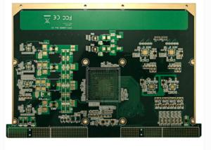
The answer involves much more than simply connecting components with copper traces. A PCB distributes power, provides controlled signal paths, establishes electrical reference and return paths, supports components mechanically, and enables circuits to perform specific functions. In many modern products, the PCB works together with integrated circuits, sensors, connectors, power-management devices, communication interfaces, and embedded firmware to form a complete electronic system.
This guide explains How Does a PCB Work, covering PCB Structure, copper layers, components, vias, traces, connectors, signal routing, power distribution, feedback circuits, and the key factors that determine PCB performance.
What Is a PCB?
A Printed Circuit Board is an engineered substrate used to mechanically support and electrically interconnect electronic components.
Unlike a simple piece of wiring, a PCB integrates conductive copper features, insulating dielectric materials, component mounting structures, and mechanical features into a defined circuit architecture.
Depending on the design requirements, PCBs can be classified into several common configurations:
- Single-Sided PCB – conductive copper features are primarily located on one side.
- Double-Sided PCB – copper circuitry is present on both sides and may be interconnected through plated holes and vias.
- Multilayer PCB – multiple copper layers are separated by dielectric materials and interconnected through plated through-holes, blind vias, buried vias, or microvias.
A PCB itself does not necessarily “receive, process, and output” information in every application. Instead, it provides the physical interconnection platform that allows components such as processors, memory devices, sensors, amplifiers, switches, and power-management circuits to perform those functions.
Therefore, understanding How Does a PCB Work requires examining both the physical PCB structure and the electronic circuit mounted on it.
PCB Structure: What Is Inside a PCB?
A typical PCB contains several functional structures. The exact construction varies according to the board type, electrical requirements, mechanical constraints, manufacturing process, and application.
The major elements include the following.
1. PCB Substrate and Dielectric Layers
The substrate provides mechanical support and electrical insulation.
For many rigid PCBs, FR-4 PCB materials based on glass-fiber reinforcement and epoxy resin are widely used. FR-4 offers a combination of mechanical strength, electrical insulation, processability, and cost effectiveness.
Other PCB materials may be selected for specialized applications.
Examples include:
- Polyimide for flexible PCBs
- High-frequency laminates for RF and microwave circuits
- Ceramic substrates for high-temperature or high-thermal-conductivity applications
- Metal-core constructions for thermal management
- High-Tg laminates for demanding thermal environments
In a multilayer PCB, dielectric materials electrically isolate adjacent copper layers while helping establish the required impedance and mechanical structure.
The dielectric thickness between a signal trace and its reference plane is particularly important for controlled-impedance and high-speed designs.
2. Copper Layers and PCB Traces
Copper is used extensively in PCB fabrication because it provides excellent electrical conductivity and can be processed into fine conductive patterns.
Depending on the PCB construction, copper may be present on:
- The top layer
- The bottom layer
- Internal signal layers
- Internal power planes
- Internal ground planes
During PCB fabrication, unwanted copper is removed or otherwise patterned to create the required circuit geometry.
The remaining copper forms PCB Traces, pads, planes, vias, and other conductive structures.
Trace characteristics such as:
- Width
- Thickness
- Length
- Spacing
- Geometry
- Reference-plane relationship
can affect current capacity, voltage drop, impedance, signal integrity, and thermal behavior.
For high-speed and RF applications, PCB traces must be designed with particular attention to impedance, return paths, electromagnetic coupling, discontinuities, and layer transitions.
This copper network is one of the most important elements in understanding How Does a PCB Work because it provides the physical paths through which electrical energy and signals travel.
3. Solder Mask
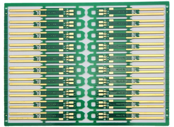
The solder mask is a protective polymer coating applied over most of the PCB’s copper surface.
The familiar green appearance of many circuit boards comes from green solder mask, although other colors are also available.
The solder mask serves several important functions:
- Helps protect exposed copper from oxidation and contamination
- Reduces the risk of accidental solder bridging
- Defines areas where soldering is intended
- Provides additional environmental protection
- Helps improve manufacturing consistency
The solder mask does not replace the PCB’s dielectric structure. Instead, it is an additional protective layer applied to the outer surfaces.
4. Electronic Components
Electronic components provide the actual circuit functions implemented on the PCB.
Depending on their package and mounting method, components are commonly divided into:
Through-Hole Components
Through-hole components have leads that pass through drilled holes in the PCB and are soldered to conductive pads.
They are often referred to as PTH components.
Through-hole technology can provide strong mechanical connections and is commonly used for certain connectors, transformers, power components, and mechanically stressed applications.
Surface-Mount Components
Surface-mount devices (SMDs) are mounted directly onto PCB pads without requiring component leads to pass through the board.
SMT allows manufacturers to achieve:
- Higher component density
- Smaller products
- Shorter electrical connections
- Automated assembly
- More compact PCB layouts
Modern PCBs commonly combine SMT and through-hole components when the application requires both technologies.
Common PCB Components and Their Functions
Different electronic components perform different electrical functions.
| Component | Typical Function |
|---|---|
| Resistor | Limits current and establishes voltage relationships |
| Capacitor | Stores and releases electrical energy; filtering and decoupling |
| Inductor | Stores energy in a magnetic field; filtering and power conversion |
| Diode | Controls current direction and provides rectification/protection |
| Transistor | Switching, amplification, and signal control |
| IC | Performs complex processing, control, memory, communication, or power-management functions |
| Crystal/Oscillator | Provides timing or clock reference |
| Sensor | Converts physical conditions into electrical signals |
| Connector | Provides electrical and mechanical interfaces to external circuits |
The PCB provides the interconnection architecture, while these components perform the electrical functions defined by the circuit design.
5. PCB Holes and Vias
Holes and vias are essential to many PCB designs.
A plated through-hole can serve both as a component mounting location and as an electrical connection between copper layers.
Vias are primarily used to establish electrical connections between different PCB layers.
Common types include:
- Through vias
- Blind vias
- Buried vias
- Microvias
Through Vias
A through via extends through the PCB and can connect multiple conductive layers.
Blind Vias
A blind via connects an outer layer to one or more internal layers without extending through the entire board.
Buried Vias
A buried via connects internal copper layers and is not directly visible from the outer surfaces.
Microvias
Microvias are typically formed using laser drilling and are widely used in HDI PCB designs to support high-density interconnection.
Vias allow signals and power to transition between layers while helping designers route increasingly complex circuits within limited board areas.
6. Connectors and Terminals
Connectors provide interfaces between the PCB and external circuits, cables, modules, batteries, displays, sensors, or other electronic assemblies.
Depending on the application, a PCB may include:
- Board-to-board connectors
- Wire-to-board connectors
- USB interfaces
- RF connectors
- Power terminals
- FFC/FPC connectors
- Card-edge connectors
These interfaces allow electrical power and signals to enter or leave the PCB.
In some applications, jumpers, wires, switches, and other external connections may also be used.
7. PCB Silkscreen
The PCB Silkscreen is a printed identification layer applied to the outer surface of the PCB.
It may contain:
- Reference designators
- Component labels
- Polarity indicators
- Pin-1 markings
- Connector labels
- Test-point identifiers
- Manufacturing information
- Warning symbols
Silkscreen does not normally participate directly in electrical conduction. Instead, it helps engineers, assembly technicians, inspectors, and repair personnel identify components and PCB features.
How Does a PCB Work?
The working principle of a PCB results from the interaction between its conductive structures, components, power sources, and signal paths.
The PCB itself does not independently “process” every input. Rather, it provides the electrical infrastructure that allows the mounted circuit to perform its intended functions.
The basic process can be understood as:
Power/Input → PCB Interconnection → Circuit Processing → Output
However, modern electronic systems may contain multiple simultaneous signal paths, power rails, feedback loops, communication interfaces, and control circuits.
Let’s examine the major mechanisms.
1. Electrical Continuity and Current Flow
Copper traces provide conductive paths between components and circuit nodes.
When a PCB assembly is connected to a power source, electrical current flows through the designed circuit according to the voltage differences, component characteristics, and circuit topology.
A properly designed PCB should provide the intended conductive paths while maintaining appropriate electrical isolation between unrelated nets.
PCB routing must therefore prevent unintended:
- Opens
- Shorts
- Excessive resistance
- Inadequate clearances
- Uncontrolled coupling
For high-current circuits, copper cross-sectional area, thermal conditions, vias, connectors, and component ratings all influence current-handling capability.
2. Power Distribution
Power distribution is a fundamental part of PCB Operation.
A PCB may contain several voltage rails, such as those required by processors, memory, analog circuits, sensors, communication interfaces, and power devices.
Power can be distributed using:
- Copper traces
- Copper pours
- Power planes
- Power vias
- Decoupling capacitors
- Power-management circuits
Ground structures provide reference and return-current paths. In high-speed designs, the quality and continuity of the return path can have a significant effect on signal integrity.
A PCB does not necessarily have dedicated power and ground layers. Their implementation depends on the board’s stackup and electrical requirements.
3. Signal Routing
PCB Signal Routing determines how electrical signals travel between components.
For example, a sensor may generate an analog signal that travels to an amplifier and then to an analog-to-digital converter. A processor may then analyze the converted data and communicate the result to another device.
A typical signal path might therefore be:
Sensor → Signal Conditioning → ADC → Processor → Communication Interface
Each section of the PCB uses specific traces, components, vias, connectors, and reference structures.
For high-speed signals, routing must also consider:
- Controlled impedance
- Differential pairs
- Return paths
- Crosstalk
- Propagation delay
- Via transitions
- Reference-plane continuity
- Electromagnetic interference
Simply connecting two components with a visible copper trace is not sufficient to guarantee good high-speed signal integrity.
4. Component Response
Every electronic component affects the electrical behavior of the circuit.
For example:
Resistors
Resistors control current and establish voltage relationships according to the circuit design.
Capacitors
Capacitors store electrical charge and are commonly used for filtering, energy storage, coupling, and power-supply decoupling.
Inductors
Inductors store energy in a magnetic field and are widely used in filters and switching power converters.
Diodes
Diodes can provide rectification, protection, signal steering, and other functions.
Transistors
Transistors can function as switches, amplifiers, regulators, and control elements.
Integrated Circuits
ICs can perform highly complex operations, including:
- Digital processing
- Analog processing
- Memory
- Communication
- Motor control
- Power management
- Data conversion
Therefore, the PCB provides the physical interconnection, while the components determine much of the circuit’s functional behavior.
5. Feedback and Control Mechanisms
Many electronic circuits use feedback to regulate their operation.
For example, a power-management circuit may measure an output voltage and compare it with a target reference. The control circuit then adjusts the power stage to maintain the desired output within the specified operating conditions.
Feedback can be found in:
- Voltage regulators
- Motor controllers
- Amplifiers
- Temperature-control systems
- Battery-management systems
- Industrial control systems
Sensors may also provide real-time information to a controller, allowing the system to respond to changes in temperature, pressure, position, current, voltage, or other physical parameters.
Therefore, feedback is not a function of the PCB substrate itself. It is a function implemented by the electronic circuit mounted on the PCB.
PCB Working Example
Consider a simple temperature-monitoring system.
The operating sequence could be:
- A temperature sensor detects the surrounding temperature.
- The sensor generates an electrical signal.
- The PCB routes the signal to a signal-conditioning circuit.
- An ADC converts the analog signal into digital data when applicable.
- A microcontroller processes the data.
- The controller compares the measured value with programmed limits.
- The system sends information to a display or communication interface.
- If the temperature exceeds a specified threshold, the controller may activate an alarm or control output.
In this example, the PCB does not perform all these operations by itself. Instead, its traces, planes, vias, components, connectors, and mechanical structure provide the infrastructure that allows the complete electronic system to perform them.
This distinction is essential when explaining How Does a PCB Work.
Factors That Affect PCB Performance
A PCB’s performance depends on much more than whether its components are electrically connected.
Important design factors include:
PCB Material
The dielectric properties, thermal characteristics, mechanical properties, and environmental resistance of the PCB material affect overall performance.
Copper Thickness
Copper thickness influences current-carrying capability, resistance, thermal behavior, and manufacturing requirements.
PCB Layer Count
Additional layers can provide more routing resources, power distribution options, and reference planes, but increasing layer count also increases manufacturing complexity and cost.
Trace Geometry
Trace width, spacing, thickness, and geometry influence impedance, resistance, current capacity, and signal integrity.
Thermal Management
Power components may generate substantial heat. Thermal vias, copper areas, heat sinks, metal-core constructions, and controlled airflow may be used depending on the application.
Component Placement
Component positioning affects signal paths, thermal distribution, electromagnetic compatibility, manufacturability, and serviceability.
Return-Path Design
High-speed signals require appropriate return-current paths. Interruptions in reference planes can create impedance discontinuities and increase electromagnetic interference.
Why Understanding PCB Operation Matters
Understanding How Does a PCB Work is useful for both PCB designers and technicians.
For designers, it helps with:
- PCB layout
- Component placement
- Power distribution
- Signal integrity
- Thermal management
- EMI/EMC considerations
- Design for Manufacturing (DFM)
- Design for Assembly (DFA)
For technicians and engineers, understanding PCB operation helps with:
- Troubleshooting
- Fault isolation
- Trace analysis
- Component testing
- PCB repair
- Reverse engineering
- Functional testing
A systematic approach is particularly useful during troubleshooting.
Instead of examining components randomly, engineers can follow the circuit from power input to functional blocks, trace signal paths, measure critical nodes, and compare measured values with the design requirements.
Future Development of PCB Technology
PCB technology continues to evolve as electronic products become smaller, faster, and more functionally integrated.
Important development directions include:
- HDI PCB technology
- Flexible and rigid-flex PCBs
- Embedded components
- Advanced high-frequency materials
- High-density packaging
- Advanced thermal-management structures
- Miniaturized interconnects
- More environmentally responsible materials and manufacturing processes
These technologies are enabling electronic products to achieve higher functionality within increasingly limited physical spaces.
At the same time, PCB design must continue to address signal integrity, thermal management, manufacturability, reliability, and sustainability.
Conclusion
So, How Does a PCB Work?
A PCB works by providing a carefully engineered platform that mechanically supports electronic components and electrically connects them through copper traces, planes, pads, vias, and other conductive structures. The PCB distributes power, establishes signal paths, provides reference and return paths, and connects different functional blocks of an electronic system.
The actual processing of electrical signals is performed by the components mounted on the board. Resistors, capacitors, inductors, diodes, transistors, sensors, processors, memory devices, and integrated circuits each perform specific functions according to the circuit design.
The combination of PCB Structure, component selection, power distribution, signal routing, grounding, thermal management, and manufacturing quality determines how effectively the complete electronic system performs.
As electronic products continue to become smaller and more sophisticated, advanced PCB Design, HDI structures, flexible circuits, high-speed routing, embedded components, and improved thermal-management technologies will become increasingly important.
For engineers, designers, and manufacturers, understanding how a PCB works is therefore more than learning how copper traces connect components. It is the foundation for designing, manufacturing, testing, troubleshooting, and improving reliable electronic products.