How Is a PCB Made? A Complete PCB Manufacturing Process
When you open a smartphone, computer, industrial controller, or household appliance, one of the most important components inside is the printed circuit board. The PCB provides the electrical pathways that connect components and enables the entire electronic system to operate as designed.
But how is a PCB actually made?
A finished circuit board is the result of a series of carefully controlled mechanical, chemical, electrical, and thermal processes. Starting with copper-clad laminate, manufacturers gradually create conductive patterns, drill interconnection holes, build copper structures, apply protective coatings, and perform electrical and visual inspections.
Understanding the PCB Manufacturing Process helps engineers and product developers better evaluate manufacturing capabilities, design requirements, quality control, and production risks.
The exact process varies according to PCB structure. A simple two-layer board may require relatively straightforward processing, while a complex Multilayer PCB or HDI PCB requires additional lamination, laser drilling, via formation, and registration processes.
Step 1: Preparing the Copper-Clad Laminate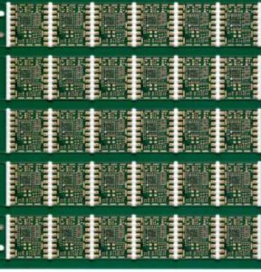
The manufacturing process begins with the base material, commonly known as copper-clad laminate (CCL).
A conventional CCL consists of an insulating substrate, often based on fiberglass-reinforced epoxy resin, with copper foil bonded to one or both sides. The substrate provides mechanical strength and electrical insulation, while the copper foil is used to form the conductive circuit patterns.
Before circuit fabrication begins, the laminate is cut according to the required production panel dimensions.
The copper surface must also be properly prepared. Cleaning and surface treatment remove dust, oxidation, oil, and other contaminants that could interfere with subsequent imaging and plating processes.
A clean and properly conditioned copper surface provides a stable foundation for creating accurate circuit patterns.
For advanced boards, material selection is particularly important. Standard FR-4 may be suitable for general applications, while high-TG, high-frequency, high-speed, flexible, and other specialized materials may be required for demanding electronic systems.
Step 2: Circuit Imaging
After the copper-clad laminate has been prepared, the circuit pattern must be transferred onto the copper surface.
One widely used approach is Laser Direct Imaging (LDI). Instead of relying on a physical photographic film, LDI uses digital circuit data to control a high-precision laser.
A photosensitive material, commonly called photoresist, is applied to the copper surface. The LDI system selectively exposes the photoresist according to the digital PCB layout.
The exposed areas undergo a chemical change, while the unexposed areas remain removable during the developing process.
After exposure, the panel enters a developing process that removes the unwanted photoresist and reveals the corresponding copper areas.
This creates a precise image of the circuit pattern on the PCB.
LDI is particularly useful for fine-line designs because it can reduce registration errors associated with conventional film-based imaging and support increasingly dense PCB layouts.
Step 3: Etching and Photoresist Stripping
Once the circuit pattern has been developed, the PCB proceeds to etching.
At this stage, portions of the copper surface that are not protected by the remaining photoresist are chemically removed.
The etching process must be carefully controlled. Excessive etching can reduce trace width, while insufficient etching may leave unwanted copper and create electrical shorts.
After the unwanted copper has been removed, the remaining photoresist is stripped away.
The result is a copper pattern consisting of traces, pads, and other conductive features that form the basic electrical network of the PCB.
For high-density boards, etching accuracy becomes increasingly important because fine traces and narrow spacing leave less process margin.
Step 4: Drilling the PCB
Drilling creates the holes required for component mounting and electrical connections between PCB layers.
Mechanical drilling is commonly used for conventional through-holes and other larger openings. Depending on the board design, additional drilling technologies may be required.
The drilling process can create:
- Through holes
- Via holes
- Component holes
- Mounting holes
- Blind vias
- Other specialized structures
For advanced Multilayer PCB designs, hole positioning must be highly accurate because the drilled holes need to align correctly with copper features on multiple internal layers.
As PCB density increases, smaller drill diameters and tighter positional tolerances become increasingly important.
For HDI structures, laser drilling can be used to create microvias that connect selected PCB layers. This enables designers to achieve higher interconnection density within a smaller board area.
Step 5: Through-Hole Plating and Copper Deposition
After drilling, the hole walls generally consist of non-conductive substrate material. Therefore, the holes must be metallized before they can provide reliable electrical connections.
A chemical copper deposition process creates an initial conductive layer on the hole walls.
This copper layer establishes electrical continuity between the surface and the drilled holes, allowing subsequent electroplating processes to build sufficient copper thickness.
Copper plating is a critical stage of PCB Fabrication because inadequate plating can lead to unreliable vias, poor electrical performance, or reduced long-term reliability.
For multilayer boards, the quality and uniformity of plated hole walls are particularly important because they provide electrical pathways between different circuit layers.
Step 6: Multilayer PCB Lamination
A Multilayer PCB is manufactured by combining multiple patterned inner layers with insulating dielectric materials and copper foil.
After individual inner layers have been fabricated and inspected, they are carefully stacked according to the specified layer structure.
Prepreg materials are placed between the conductive layers. Under controlled temperature and pressure, the materials are laminated together into a solid multilayer structure.
During lamination, several parameters must be controlled, including:
- Temperature
- Pressure
- Heating and cooling rates
- Resin flow
- Layer alignment
- Material thickness
Layer registration is particularly important. Even a small alignment error can affect vias, pads, traces, and other features.
The resulting multilayer panel forms a three-dimensional electrical structure in which different layers perform signal, power, and ground functions.
Step 7: Outer-Layer Circuit Formation
Once the multilayer structure has been laminated and drilled, the outer copper layers are processed to create the final external circuit pattern.
Similar imaging, developing, plating, and etching principles are used to form the required traces and pads.
Depending on the design, additional copper may be electroplated onto selected areas to achieve the required conductor thickness.
For high-current applications, manufacturers may use heavier copper structures to improve current-carrying capability and thermal performance.
For high-speed designs, trace geometry and layer structure must also be carefully controlled to maintain signal integrity and impedance requirements.
Step 8: Solder Mask Application
After the conductive circuitry has been completed, the PCB receives a solder mask layer.
The solder mask is a protective coating that covers most of the copper surface while leaving selected soldering areas exposed.
It serves several important purposes:
- Protects copper from oxidation
- Reduces the risk of accidental short circuits
- Protects the circuit from environmental contamination
- Helps prevent solder bridges during assembly
- Improves the overall durability of the PCB
Green is the most familiar solder mask color, but other colors such as black, blue, red, white, and matte finishes may also be available depending on manufacturing requirements.
The solder mask is normally applied, exposed, developed, and cured to create openings precisely over the required pads.
The accuracy of these openings is important because the exposed pad area must correspond correctly with the component footprint used during PCB assembly.
Step 9: Silkscreen Printing
After solder mask processing, manufacturers may apply silkscreen markings to the PCB surface.
Silkscreen typically contains reference designators, polarity indicators, logos, labels, test-point markings, and other information used during assembly and maintenance.
Examples include:
- R1 for a resistor
- C1 for a capacitor
- U1 for an integrated circuit
- Connector identification
- Pin-1 indicators
- Warning labels
Clear silkscreen information makes component placement easier during assembly and can also simplify troubleshooting and maintenance later in the product lifecycle.
Step 10: PCB Surface Finishing
The exposed copper pads require additional surface protection before the PCB can be assembled.
Without an appropriate surface finish, exposed copper can oxidize and may become less suitable for soldering.
Common PCB surface finishes include:
HASL
Hot Air Solder Leveling applies solder to exposed copper pads and removes excess solder using hot air.
It is widely used for general PCB applications and can provide good solderability at a relatively economical cost.
ENIG
Electroless Nickel Immersion Gold provides a relatively flat surface and is commonly selected for fine-pitch components, high-density designs, and applications where a stable solderable surface is required.
OSP
Organic Solderability Preservative protects exposed copper with a thin organic coating. It can be a cost-effective option for many PCB assembly applications.
Immersion Silver and Immersion Tin
These finishes provide alternative surface protection and solderability characteristics for specific manufacturing requirements.
The appropriate finish should be selected according to component type, assembly process, environmental conditions, reliability requirements, and product cost targets.
Step 11: Electrical and Visual Inspection
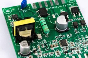
Manufacturing is not complete when the physical PCB has been fabricated. Each board must undergo appropriate inspection and testing.
Visual inspection can identify problems such as:
- Scratches
- Copper exposure
- Solder mask defects
- Surface contamination
- Incorrect silkscreen
- Dimensional abnormalities
- Visible circuit defects
Automated Optical Inspection (AOI) can be used to inspect circuit patterns and identify potential opens, shorts, missing features, and other manufacturing defects.
Electrical testing verifies the integrity of the circuit connections and insulation. Depending on production requirements, manufacturers may use flying probe testing or fixture-based electrical testing.
For high-speed and controlled-impedance designs, impedance testing can also be performed to verify that critical transmission lines meet the specified electrical requirements.
For customers looking for a complete PCB Manufacturing solution, integrating fabrication with appropriate inspection and quality-control procedures can provide a more consistent production workflow.
Step 12: PCB Final Inspection and Packaging
After electrical testing, qualified boards undergo final inspection before shipment.
Final inspection may verify:
- Board dimensions
- Thickness
- Hole sizes
- Copper features
- Surface finish
- Solder mask
- Silkscreen
- Electrical test results
- Packaging requirements
The finished PCBs are then cleaned and packaged appropriately to protect them from moisture, contamination, mechanical damage, and electrostatic risks during storage and transportation.
Packaging requirements may vary depending on the PCB material, surface finish, application, and customer’s storage conditions.
How Does HDI PCB Manufacturing Differ?
An HDI PCB requires additional processes compared with conventional multilayer boards.
HDI technology can incorporate microvias, blind vias, buried vias, fine-line structures, and sequential build-up layers.
Laser drilling is commonly used to create microvias, while sequential lamination may be required to build the board structure layer by layer.
The main objective is to increase interconnection density without continuously increasing the physical dimensions of the PCB.
HDI technology is particularly useful for compact electronic products, communication equipment, automotive electronics, medical devices, computing systems, and other applications where PCB space is limited.
Because HDI structures involve smaller features and tighter registration requirements, material selection, laser drilling, lamination, copper plating, and inspection all require careful process control.
PCB Assembly After Fabrication
The finished bare PCB is only the foundation of an electronic product. Components such as integrated circuits, resistors, capacitors, connectors, and sensors must still be mounted and soldered onto the board.
Depending on the product, assembly may use Surface Mount Technology (SMT), Through-Hole Technology (THT), or a combination of both.
Prototype projects often require fast assembly and engineering feedback because the assembled board is used to validate the design.
GOPCBA provides Prototype PCB Assembly services to support prototype development, assembly, inspection, and design validation.
For production programs, PCB fabrication and assembly can also be coordinated as part of a broader electronics manufacturing workflow.
Why PCB Manufacturing Quality Matters
Every stage of the PCB Manufacturing Process contributes to the performance and reliability of the finished board.
A problem during imaging can affect trace geometry. Poor etching can cause opens or shorts. Incorrect drilling can compromise vias. Inadequate copper plating can reduce interconnection reliability. Poor lamination can affect multilayer registration and structural integrity.
Similarly, inappropriate surface finishing or solder mask processing can create assembly and reliability problems.
For this reason, PCB manufacturing should be viewed as an integrated process rather than a collection of unrelated production steps.
Engineering review, material selection, process control, inspection, and electrical testing all work together to ensure that the final PCB meets the original design requirements.
How to Improve PCB Manufacturing Efficiency
Efficient PCB production begins before fabrication.
Optimize the PCB Design
A manufacturing-friendly PCB layout can reduce unnecessary process complexity and improve production yield.
Engineers should consider trace width, spacing, hole sizes, component clearances, copper distribution, layer stack-up, and material selection during the design stage.
Perform DFM Review
Design for Manufacturing review can identify potential production problems before the design reaches the factory.
This is especially valuable for HDI, high-speed, multilayer, rigid-flex, and other advanced PCB designs.
Select Materials Carefully
The PCB material should match the electrical, thermal, mechanical, and environmental requirements of the application.
Using a material that is unsuitable for the operating conditions can create reliability problems even when the manufacturing process itself is correct.
Integrate PCB and PCBA Services
Managing PCB fabrication and assembly through multiple unrelated suppliers can increase communication and logistics complexity.
An integrated manufacturing workflow can simplify coordination between PCB production, component sourcing, assembly, inspection, and delivery.
GOPCBA also provides Components Procurement services to help coordinate electronic component sourcing with PCBA production requirements.
From PCB Prototype to Volume Production
The manufacturing process may change depending on the stage of product development.
During prototype development, the main priorities are often engineering validation, rapid turnaround, and design flexibility.
During low-volume production, manufacturers need to balance production efficiency, quality, and cost.
When a product enters high-volume production, process stability, automation, material availability, yield, and production consistency become increasingly important.
Choosing a manufacturing partner that can support multiple stages can make the transition from prototype to production more efficient.
For projects requiring a complete electronics manufacturing workflow, Turnkey PCB Assembly can combine component procurement, PCB assembly, testing, and delivery into a coordinated service.
Conclusion
So, how is a PCB made?
The answer involves a carefully controlled sequence of processes, beginning with copper-clad laminate preparation and continuing through circuit imaging, etching, drilling, copper plating, lamination, solder mask application, silkscreen printing, surface finishing, electrical testing, and final inspection.
For simple boards, the process may be relatively straightforward. For advanced Multilayer PCB and HDI PCB designs, additional technologies such as sequential lamination, laser drilling, microvias, controlled impedance, and advanced inspection may be required.
A professional PCB manufacturing partner should therefore offer not only strong PCB Fabrication capabilities but also engineering support, quality management, flexible production, and assembly integration.
By understanding the complete PCB Manufacturing Process, engineers and purchasing teams can make better decisions when selecting materials, designing boards, evaluating suppliers, and planning production from prototype through volume manufacturing.