Drone Swarm Communication PCB: Design, Performance and Manufacturing Requirements
Drone swarm technology depends on fast, stable, and reliable communication between multiple unmanned aerial vehicles. Whether used for coordinated surveillance, emergency response, environmental monitoring, logistics, or other demanding applications, every drone in a swarm must exchange commands, positioning information, sensor data, and status information with minimal delay.
At the center of this communication architecture is the Drone Swarm Communication PCB. As the physical platform connecting communication processors, RF modules, antennas, power circuits, sensors, and other electronic components, the PCB directly affects signal integrity, system reliability, electromagnetic compatibility, and overall communication performance.
As drone systems become smaller while requiring greater computing and communication capabilities, communication PCBs must provide high circuit density, reliable signal transmission, strong environmental resistance, and optimized thermal and mechanical performance.
What Is a Drone Swarm Communication PCB?
A Drone Swarm Communication PCB is a specialized printed circuit board designed to support communication and data-processing functions within unmanned aerial systems operating as part of a coordinated network.
Unlike conventional electronic control boards, drone communication PCBs often need to integrate high-speed digital circuits, RF communication modules, antenna interfaces, power management circuits, processors, and sensor interfaces within a compact form factor.
The PCB must provide stable electrical connections while minimizing signal loss, electromagnetic interference, crosstalk, and unwanted noise.
In a multi-drone network, communication reliability becomes particularly important because the performance of one communication node can influence the coordination of the entire system.
Key Functions of Drone Swarm Communication PCBs
High-Speed Data Transmission
A drone swarm may need to exchange positioning information, telemetry, sensor data, images, video streams, and control information in real time.
The PCB must therefore support high-speed interfaces and carefully controlled signal paths. Trace geometry, impedance control, dielectric characteristics, layer configuration, and connector design can all affect signal quality.
For demanding communication applications, a carefully engineered High-Frequency PCB structure can help reduce transmission losses and maintain signal integrity at higher operating frequencies.
Compact Circuit Integration
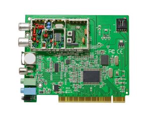
Weight and available installation space are major considerations in drone design. Communication electronics must provide high functionality without adding unnecessary size or weight.
Multilayer PCB technology allows designers to integrate signal, power, ground, and communication circuits into a compact structure. Proper layer stacking can also improve electromagnetic performance while reducing routing congestion.
High-density layouts can accommodate processors, RF components, memory devices, connectors, and power circuits while maintaining controlled electrical characteristics.
Power Distribution
Communication modules, processors, RF circuits, sensors, and other electronics require stable power.
The communication PCB must distribute power efficiently while minimizing voltage fluctuations and electrical noise. Proper power-plane design, grounding strategies, decoupling components, and thermal management are therefore essential.
A well-designed power distribution structure can help prevent communication instability caused by voltage noise or transient interference.
Critical Performance Requirements
Drone swarm communication systems can operate in environments with significant temperature changes, vibration, electromagnetic interference, and mechanical stress. The PCB must therefore be designed around the actual operating conditions rather than only laboratory conditions.
Electromagnetic Interference Resistance
Electromagnetic interference is one of the most important challenges for wireless communication electronics.
Nearby RF modules, processors, motors, power converters, antennas, and other electronic systems can generate electromagnetic noise. Without appropriate PCB design, interference can affect sensitive communication signals and reduce system reliability.
Common PCB design approaches include:
- Optimized grounding structures
- Controlled impedance routing
- Differential signal routing
- Appropriate separation between RF and digital circuits
- Ground planes and shielding structures
- Short and direct high-speed signal paths
- Careful placement of sensitive components
- Controlled return-current paths
These measures can reduce unwanted coupling and improve electromagnetic compatibility.
Wide Temperature Stability
Drone systems may operate across significant temperature variations depending on altitude, geographical location, operating duration, and mission conditions.
PCB materials and components must maintain stable electrical and mechanical properties across the expected operating temperature range.
Important considerations include:
- Glass transition temperature of the laminate
- Coefficient of thermal expansion
- Copper-to-laminate adhesion
- Component temperature ratings
- Solder joint reliability
- Thermal cycling performance
- Moisture resistance
Selecting suitable materials at the design stage can significantly improve long-term reliability.
Vibration and Mechanical Reliability
During flight, drones experience continuous vibration generated by motors, propellers, aerodynamic forces, landing impacts, and changes in flight conditions.
Repeated mechanical stress can affect solder joints, connectors, components, and PCB structures.
To improve mechanical reliability, engineers may optimize PCB mounting points, reinforce heavy components, minimize mechanical stress around connectors, and select appropriate assembly processes.
The PCB thickness, mounting structure, component placement, and enclosure design should also be considered together rather than independently.
PCB Materials for Communication Applications
Material selection has a direct influence on communication performance.
For high-speed and RF applications, designers may consider laminates with stable dielectric properties and low dielectric loss. These characteristics can help maintain signal integrity and reduce transmission losses.
Material selection should consider:
- Dielectric constant
- Dissipation factor
- Thermal stability
- Moisture absorption
- Dimensional stability
- Mechanical strength
- Copper adhesion
- Operating frequency
For complex designs, hybrid material structures may also be considered when different circuit sections have different electrical requirements.
The material should always be selected according to the actual frequency, temperature, mechanical, and environmental requirements of the application.
PCB Layout Considerations for Drone Communication Systems
Controlled Impedance Routing
High-speed digital and RF signals require carefully controlled transmission lines.
Trace width, copper thickness, dielectric thickness, layer structure, and dielectric constant all influence impedance.
Impedance-controlled routing is especially important for RF interfaces and high-speed differential signals. PCB designers should establish the target impedance before routing and maintain consistent geometry throughout the signal path.
Signal Integrity
Signal integrity becomes increasingly important as communication frequencies and data rates increase.
Designers should pay attention to:
- Trace length
- Return paths
- Via transitions
- Differential-pair spacing
- Crosstalk
- Ground-plane continuity
- Connector characteristics
- Layer transitions
Avoiding unnecessary routing changes and minimizing discontinuities can improve high-speed performance.
Thermal Management
Processors, RF power amplifiers, voltage regulators, and other components can generate considerable heat.
PCB thermal management may involve:
- Thermal vias
- Copper planes
- Larger copper areas
- Heat sinks
- Optimized component placement
- Improved airflow
- Thermal interface structures
Thermal design should be evaluated together with the mechanical enclosure and overall drone architecture.
Manufacturing Requirements for Drone Communication PCBs
A high-performance design can only deliver reliable results when the manufacturing process maintains the required dimensional, electrical, and material specifications.
Professional PCB Manufacturing requires close control over materials, layer alignment, drilling, copper plating, etching, solder mask, surface finish, electrical testing, and final inspection.
Precision Drilling and Via Structures
Modern communication boards may contain small vias, fine-pitch components, microvias, blind vias, or buried vias.
Drilling accuracy is important because dimensional deviations can affect layer registration, impedance, connectivity, and assembly reliability.
For high-density communication designs, manufacturing capabilities should be evaluated based on the actual via diameter, aspect ratio, layer count, registration tolerance, and interconnection structure required by the design.
Copper Plating and Trace Quality
Copper thickness and plating quality directly affect electrical performance and reliability.
Uniform copper deposition is important for maintaining consistent conductor dimensions and reliable interlayer connections.
Manufacturing controls should monitor copper thickness, plating uniformity, hole-wall quality, and surface condition.
Surface Finish
The surface finish must be compatible with the selected components and assembly process.
Common options include ENIG, HASL, OSP, and other finishes. Selection should consider solderability, storage requirements, environmental conditions, fine-pitch assembly requirements, and expected product life.
PCB Assembly for Drone Communication Electronics
After PCB fabrication, component assembly becomes another critical stage.
Communication boards may contain fine-pitch ICs, RF components, BGA packages, small passive components, connectors, and power-management devices. These components require accurate placement and consistent soldering.
Modern PCB Assembly processes typically integrate automated component placement, solder paste printing, reflow soldering, inspection, and electrical testing.
SMT Assembly
Surface mount technology is particularly suitable for compact drone communication electronics because it enables high component density and automated manufacturing.
Important SMT manufacturing factors include:
- Solder paste consistency
- Stencil design
- Component placement accuracy
- Reflow temperature profile
- BGA solder-joint quality
- Fine-pitch component inspection
- Automated optical inspection
For high-density boards, process optimization is essential to reduce solder defects and maintain consistent production quality.
Component Procurement
Communication systems often require specialized processors, RF components, connectors, power-management ICs, memory devices, and other electronic components.
Reliable Components Procurement is therefore an important part of the overall manufacturing process.
Component sourcing should consider manufacturer authenticity, availability, lifecycle status, specifications, traceability, and supply continuity.
Using verified components can reduce the risks associated with counterfeit parts, unexpected substitutions, and long-term supply interruptions.
Prototype Development and Testing
Before entering volume production, prototype development allows engineers to validate the PCB design, communication performance, mechanical integration, and assembly process.
Prototype PCB Assembly is particularly useful when developing a new drone communication platform because it allows design teams to identify potential issues before committing to larger production quantities.
Prototype testing may include:
- Electrical continuity testing
- Functional testing
- RF performance verification
- Signal integrity testing
- Thermal testing
- Vibration testing
- Connector and mechanical testing
- Electromagnetic compatibility evaluation
Testing should be based on the actual application requirements and expected operating environment.
From Prototype to Low-Volume Production
After prototype validation, many drone communication products initially enter low-volume production.
This stage is useful for field trials, engineering validation, customer evaluation, and early-stage deployment.
Low-Volume PCB Assembly allows manufacturers to support smaller production quantities while maintaining controlled assembly quality.
A structured transition from prototype to low-volume production should include:
- Design verification
- BOM validation
- Component availability confirmation
- PCB manufacturing review
- Assembly process optimization
- Functional testing
- Reliability verification
- Production documentation
- Quality inspection
- Feedback for subsequent design revisions
This approach helps reduce manufacturing risks while providing flexibility during product development.
Applications of Drone Swarm Communication PCBs
Drone communication PCBs can support a wide range of civilian and industrial applications.
Emergency Response
Multiple drones can cooperate to collect aerial images, locate targets, monitor affected areas, and transmit information to a centralized command system.
Reliable communication electronics are essential for maintaining connectivity among drones and ground-based systems.
Agriculture and Environmental Monitoring
Drone fleets can coordinate flight paths, collect environmental data, monitor crops, and perform large-area inspections.
Communication PCBs help synchronize data and maintain connectivity between individual aircraft and control stations.
Infrastructure Inspection
Coordinated drones can be used for inspection of power infrastructure, bridges, construction sites, industrial facilities, and other large areas.
High-speed communication can help transmit sensor data and high-resolution imagery efficiently.
Logistics and Automated Operations
In logistics applications, networked drones may exchange location and operational information to improve fleet coordination.
Reliable communication electronics help support route management, status monitoring, and centralized fleet control.
How to Choose a PCB and PCBA Partner
When selecting a manufacturing partner for drone communication electronics, price should not be the only consideration.
Important evaluation factors include:
- PCB manufacturing capabilities
- High-frequency and high-speed PCB experience
- Fine-pitch SMT assembly capability
- Component sourcing and traceability
- Prototype support
- Low-volume production capabilities
- Electrical and functional testing
- Quality management systems
- Engineering support
- Production scalability
A manufacturer that can support PCB fabrication, component sourcing, assembly, and testing through an integrated workflow can simplify project management and reduce communication gaps between suppliers.
Conclusion
The Drone Swarm Communication PCB is a critical foundation for reliable multi-drone communication systems. As drone platforms become smaller, faster, and more connected, their communication electronics must provide higher circuit density, better signal integrity, improved electromagnetic compatibility, thermal stability, and mechanical reliability.
Successful development requires more than simply designing a circuit board. Material selection, PCB layout, impedance control, manufacturing precision, component procurement, SMT assembly, testing, and reliability verification must all work together.
For engineering teams developing next-generation drone communication systems, working with an experienced PCB and PCBA manufacturing partner can help turn complex communication designs into reliable production-ready electronics.