Custom PCB for Power Monitoring Systems
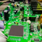
As power systems continue to evolve toward greater intelligence, automation, and digitalization, power monitoring systems function as the sensing and communication center of modern electrical networks. They continuously capture changes in voltage, current, temperature, and other operating parameters. At the hardware level, a Custom PCB for Power Monitoring Systems provides the electrical foundation for these functions.
Unlike standard circuit boards designed for general-purpose electronics, power monitoring PCBs must be adapted to specific electrical, environmental, mechanical, and integration requirements. A properly engineered Power Monitoring PCB can improve electromagnetic compatibility, thermal stability, signal integrity, mechanical reliability, and long-term operational performance.
For demanding applications, manufacturers can combine appropriate materials, multilayer structures, grounding strategies, controlled impedance, copper thickness, and protective processes to create a PCB optimized for the actual operating environment.
Core Customization Requirements for Power Monitoring PCBs
Power monitoring equipment may operate continuously in environments exposed to strong electromagnetic interference, temperature fluctuations, humidity, vibration, and electrical transients. These conditions place significantly higher requirements on PCB design and manufacturing than many conventional consumer electronics applications.
Electromagnetic Interference Protection
Electromagnetic interference resistance is one of the most important considerations when developing a Power Monitoring PCB. In substations, distribution rooms, and other electrical facilities, high-voltage equipment can generate electromagnetic fields that interfere with sensitive measurement and communication circuits.
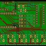
A customized PCB can incorporate carefully designed ground planes, power distribution structures, signal routing, and shielding strategies. In multilayer constructions, dedicated ground and power planes can help isolate sensitive signal paths and reduce unwanted coupling.
Proper grounding and routing are particularly important for circuits responsible for acquiring low-level voltage, current, temperature, or sensor signals. A well-engineered structure can help maintain measurement accuracy while reducing the risk of noise-induced communication or monitoring errors.
Thermal Stability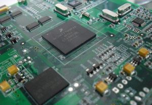
Temperature resistance is another critical requirement for power monitoring equipment. Outdoor installations, substations, and equipment cabinets may experience substantial temperature changes throughout the year. Repeated thermal expansion and contraction can place mechanical stress on the PCB and its interconnections.
High-Tg laminate materials may be selected for applications requiring improved thermal stability. Material selection should be coordinated with the expected operating temperature, copper structure, board thickness, layer count, and assembly process.
For complex applications, the PCB stack-up and lamination process should also be carefully controlled to minimize dimensional changes, delamination risks, and warpage.
Appropriate PCB Materials can therefore play an important role in maintaining long-term electrical and mechanical stability under demanding operating conditions.
Moisture and Corrosion Protection
Moisture and corrosion protection can be essential for monitoring equipment installed in coastal regions, industrial facilities, outdoor cabinets, or other humid environments.
High humidity and salt contamination can accelerate copper oxidation and potentially reduce the reliability of exposed conductive surfaces. Depending on the application, protective coatings, suitable surface finishes, optimized solder mask processes, and appropriate enclosure design can be used to improve environmental resistance.
The protection strategy should be selected according to the actual operating environment rather than applied as a one-size-fits-all solution.
PCB Customization for Different Power Monitoring Applications
Different power monitoring environments place different demands on PCB structure, mechanical design, electrical performance, and environmental protection. Custom PCB engineering allows the board architecture to be optimized for each application.
High-Voltage Transmission Line Monitoring Terminals
Monitoring equipment installed on transmission towers must withstand wind, vibration, rain, temperature changes, and long-term outdoor exposure.
The PCB may therefore require enhanced mechanical strength and environmental protection. Board thickness, mounting-hole design, component placement, solder-joint reliability, and enclosure integration should be considered together.
For applications involving mechanical movement or constrained installation spaces, rigid-flex or flexible PCB structures may provide additional design flexibility. Properly engineered mechanical transitions can help accommodate limited movement while maintaining electrical continuity.
Intelligent Distribution Room Monitoring Units
Distribution rooms often contain multiple electrical devices and monitoring functions within limited installation space. The monitoring unit may need to interface with current transformers, voltage sensors, temperature sensors, humidity sensors, communication interfaces, and other peripherals.
A customized multilayer structure can integrate multiple functional circuits into a compact board while maintaining appropriate isolation and signal-routing strategies.
Using a Multilayer PCB can reduce external wiring and improve system integration. Separate signal, power, and ground structures can also help organize complex circuits and reduce electromagnetic coupling.
For compact monitoring equipment, PCB layout must balance component density, thermal management, creepage and clearance requirements, serviceability, and manufacturing feasibility.
Renewable Energy Monitoring Equipment
Solar power plants, wind farms, energy storage systems, and other renewable energy installations increasingly rely on electronic monitoring and control systems.
These systems may require low standby power, reliable sensor acquisition, communication interfaces, and stable operation under changing environmental conditions. PCB design can be optimized by reducing unnecessary power losses, shortening current paths, and selecting components and materials appropriate for the application.
For renewable energy equipment that handles both power electronics and sensitive monitoring signals, thermal management and electromagnetic compatibility should be considered from the earliest design stage.
Manufacturing Processes for Reliable Power Monitoring PCBs
A reliable PCB for power monitoring applications requires more than an appropriate schematic and layout. Manufacturing consistency is equally important because dimensional variation, material changes, drilling accuracy, copper thickness, and layer registration can influence final electrical performance.
Material Selection and Lamination
Material selection should be based on electrical, thermal, mechanical, and environmental requirements. Standard FR-4 may be suitable for many applications, while high-Tg materials or other specialized laminates may be appropriate for more demanding environments.
For multilayer boards, lamination parameters must be carefully controlled. Temperature, pressure, heating rate, cooling rate, resin flow, and layer alignment can affect dielectric thickness, bonding quality, dimensional stability, and final board reliability.
Precision PCB Drilling and Copper Plating
Plated through-holes provide electrical connections between conductive layers in multilayer boards. Their reliability is particularly important when monitoring equipment contains multiple power and signal layers.
During fabrication, controlled drilling, hole-wall preparation, electroless copper deposition, and electrolytic copper plating help establish reliable interlayer connections.
For higher-current applications, copper thickness and via structure should be designed according to the required current capacity and thermal conditions. Proper copper distribution can also help reduce localized heating.
Electrical Testing and Quality Inspection
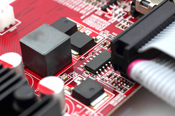
Quality control should cover both manufacturing defects and electrical performance. Depending on the project, inspection may include automated optical inspection, dimensional inspection, X-ray inspection, cross-section analysis, and electrical testing.
100% electrical testing can help verify circuit continuity, insulation, and overall electrical integrity before shipment.
For complex boards, engineering review and DFM analysis before production can further reduce manufacturing risks and identify potential problems with spacing, drilling, layer registration, stack-up, or component integration.
Signal Integrity and Controlled Impedance
Power monitoring systems increasingly combine conventional power measurement with digital communication, remote monitoring, and high-speed data interfaces. As a result, signal integrity can become an important part of PCB engineering.
A Controlled Impedance PCB maintains predictable transmission-line characteristics by controlling parameters such as trace width, copper thickness, dielectric thickness, dielectric constant, and reference-plane configuration.
For sensitive communication interfaces, impedance-controlled routing can help reduce signal reflection and maintain more consistent transmission characteristics.
The PCB manufacturer and design engineers should therefore coordinate stack-up construction, material selection, trace geometry, and manufacturing tolerances before production. This is especially important for multilayer monitoring boards that combine high-speed digital signals with power circuits and low-level analog measurement channels.
How Custom PCBs Improve Power Monitoring System Performance
A customized PCB should be considered part of the overall power monitoring architecture rather than an isolated hardware component.
At the data acquisition level, optimized grounding, routing, shielding, and signal conditioning can help preserve measurement accuracy. At the communication level, controlled impedance and carefully designed reference planes can support stable data transmission.
At the mechanical level, customized board dimensions, mounting structures, connector positions, and component layouts allow the PCB to fit the equipment enclosure more efficiently.
For development projects, PCB Prototype Manufacturing can also provide an important validation stage before production. Prototype boards allow engineers to evaluate electrical performance, thermal behavior, mechanical integration, signal quality, and manufacturability before committing to larger production volumes.
Modular PCB architecture can further simplify maintenance. When a monitoring unit experiences a failure, individual functional boards or modules can potentially be replaced instead of replacing the complete equipment assembly. This approach can reduce maintenance time and improve system serviceability.
Conclusion
Custom PCB engineering is an important part of developing reliable power monitoring systems for substations, transmission networks, distribution facilities, renewable energy installations, and industrial electrical equipment.
The most effective approach combines appropriate materials, electromagnetic compatibility strategies, thermal management, environmental protection, multilayer construction, reliable interlayer connections, controlled impedance, and systematic quality inspection.
As power infrastructure becomes increasingly digital and intelligent, PCB requirements will continue to evolve toward higher integration, improved reliability, stronger signal integrity, and greater environmental adaptability. A professionally engineered Power Monitoring PCB can provide the stable hardware foundation required for accurate data acquisition, dependable communication, and long-term system operation.