How to Detect a Short Circuit on a PCB: PCB Testing, Troubleshooting & Prevention
Printed circuit boards (PCBs) have become essential components in almost every modern electronic product. As manufacturers continue to integrate more intelligent functions into individual devices, electronic circuits are becoming increasingly complex while simultaneously becoming smaller and more compact. To accommodate higher component density and more advanced functionality, PCB design has evolved from simple single-layer boards to compact multilayer structures with highly sophisticated interconnections.
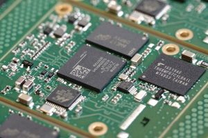
From a system perspective, even a small PCB board can contain an extremely large and complex circuit. Very-large-scale integration (VLSI) and ultra-large-scale integration (ULSI) technologies allow millions of transistors and electronic functions to be integrated into compact devices. As a result, the complexity of modern PCB manufacturing and assembly has increased significantly, making design accuracy, manufacturing quality, inspection, and troubleshooting more important than ever.
During PCB manufacturing, assembly, installation, operation, and maintenance, various electrical and physical defects can occur. Among them, a short circuit is one of the most critical problems because it can cause excessive current, component damage, overheating, malfunction, and, in severe cases, complete system failure.
Therefore, understanding how to detect a short circuit on a PCB is essential for engineers, technicians, manufacturers, and maintenance personnel. This guide explains the causes and symptoms of PCB short circuits, introduces common and advanced PCB testing methods, and provides practical strategies for preventing short circuits during design and production.
What Is a Short Circuit on a PCB?
A short circuit on a PCB occurs when two electrical nodes, nets, traces, pads, pins, or conductive areas that should remain electrically isolated become unintentionally connected.
Under normal operating conditions, electrical current follows a predetermined path defined by the circuit design. When an unintended conductive path is created, current may bypass the intended circuit and flow through a low-resistance path.
Depending on the location and severity of the short circuit, the resulting problems may include:
- Excessive current flow
- Abnormal voltage levels
- Component overheating
- Damaged ICs and semiconductor devices
- Blown fuses or protection components
- Power supply shutdown
- Signal distortion or loss
- Intermittent system failures
- Permanent PCB board damage
- In severe cases, thermal damage or fire hazards
Short circuits can occur during the PCB design, fabrication, soldering, assembly, installation, or repair stages. Identifying the root cause is therefore just as important as detecting the short itself.
Common Causes of PCB Short Circuits
A short circuit can originate from either design-related problems or manufacturing and assembly defects. The most common causes include the following.
1. PCB Design Errors
Improper PCB design is one of the earliest potential sources of short circuits. Insufficient spacing between copper traces, incorrect routing, overlapping traces, incorrect net assignments, or improperly designed vias can create unintended electrical connections.
Designers should carefully check:
- Trace-to-trace clearance
- Pad-to-pad spacing
- Via-to-via clearance
- Copper-to-edge clearance
- High-voltage creepage and clearance
- Ground and power routing
- Multilayer stackup connections
Using Design Rule Check (DRC) and Electrical Rule Check (ERC) before releasing manufacturing files can significantly reduce design-related risks.
2. Excessive Solder and Solder Bridges
During PCB assembly, excessive solder can connect adjacent pads, pins, or copper traces. This creates a conductive bridge commonly known as a solder bridge.
Solder bridges are particularly common with fine-pitch surface-mount components, where the distance between adjacent pins can be extremely small.
Poor solder paste application, incorrect stencil design, excessive solder volume, or inappropriate reflow parameters can all increase the risk.
3. Component Misalignment
Components must be positioned accurately on their designated pads. If a component shifts during placement or soldering, its leads or terminals may contact nearby traces or pads.
This problem can occur because of:
- Incorrect component placement
- Excessive solder paste
- Poor component orientation
- Inaccurate pick-and-place settings
- PCB warpage
- Incorrect pad design
Automated optical inspection can help identify many of these problems before the assembled board reaches the customer.
4. Conductive Contamination
A PCB operating in an environment with high humidity, dust, chemicals, or conductive contaminants may develop unintended electrical paths across its surface.
Flux residues, metal particles, dust, moisture, and other contaminants can reduce surface insulation resistance. In extreme conditions, they may contribute to leakage currents or electrical shorts.
Proper cleaning, conformal coating, environmental protection, and appropriate material selection can reduce these risks.
5. Multilayer PCB Connection Errors
Multilayer PCB boards contain multiple copper layers separated by dielectric materials. Vias and other interconnections are used to connect specific layers.
An incorrectly positioned via, incorrect drill, unwanted copper connection, or stackup error can connect two nets that should remain isolated.
Because these defects may be hidden inside the board, multilayer PCB short circuits can be much more difficult to locate than surface-level defects.
6. Repair and Rework Errors
During PCB repair, engineers may add jumper wires, modify traces, replace components, or remove damaged copper.
If a jumper wire is incorrectly connected or a repaired trace is routed too close to another conductor, an unintended short circuit may occur.
For this reason, repaired boards should undergo electrical testing before returning to service.
Symptoms of a PCB Short Circuit
Recognizing abnormal behavior is an important part of PCB troubleshooting. A short circuit may produce obvious symptoms, although some shorts can be intermittent or difficult to identify.
Common warning signs include:
- The device fails to power on.
- The power supply enters protection mode.
- A fuse repeatedly blows.
- An IC or component becomes unusually hot.
- A specific area of the PCB develops a localized hot spot.
- There is an unusual burning smell.
- The power supply current is significantly higher than expected.
- Voltage measurements are abnormal.
- The system resets unexpectedly.
- Communication signals disappear or become unstable.
- Components fail immediately after power is applied.
A sudden increase in current consumption is particularly useful during initial diagnosis. However, not every abnormal current condition is necessarily caused by a hard short. Partial shorts, leakage paths, damaged components, and incorrect circuit operation can produce similar symptoms.
Therefore, systematic PCB testing is recommended rather than relying on a single observation.
How to Detect a Short Circuit on a PCB
There are several ways to detect a short circuit, ranging from simple visual inspection to sophisticated automated and non-destructive testing technologies.
The appropriate method depends on the board’s complexity, layer count, component density, production volume, and the location of the suspected defect.
1. Visual Inspection
Visual inspection is one of the simplest and fastest methods for identifying surface-level PCB defects.
Technicians can inspect the board under sufficient lighting and use magnification to look for:
- Solder bridges
- Solder splashes
- Misaligned components
- Damaged traces
- Burn marks
- Copper debris
- Foreign conductive particles
- Incorrect jumper wires
- Damaged pads
- Improper rework
A microscope or digital inspection camera is especially useful for high-density PCB assembly, where small solder bridges may not be visible to the naked eye.
Changing the viewing angle and using directional lighting can also reveal surface contamination and solder-related defects.
For densely populated boards, inspection may need to be performed before and after component installation to ensure that defects hidden beneath components are not overlooked.
2. Manual Testing with a Multimeter
A digital multimeter is one of the most practical tools for PCB troubleshooting.
Before performing resistance or continuity measurements, the PCB should normally be disconnected from the power source. Measuring resistance on an energized circuit can produce inaccurate results and may damage the meter or circuit.
Continuity Test
Set the multimeter to continuity mode and place the probes across two points that should not normally be electrically connected.
If the meter produces a continuous beep or indicates very low resistance, there may be an unintended connection.
However, engineers should interpret continuity measurements carefully because some circuits naturally contain low-resistance paths through components, power planes, coils, semiconductor devices, or protection circuits.
Resistance Measurement
Resistance measurement can provide additional information.
A very low resistance between two isolated nets can indicate a possible short circuit. Engineers can compare the measured value with the expected resistance based on the schematic and known circuit topology.
For example, if a power rail and ground are expected to be electrically isolated but the meter shows an unusually low resistance, further investigation is required.
Important Consideration
Some capacitors initially appear as short circuits when measured with a multimeter because they charge during the measurement. Therefore, a single resistance reading should not automatically be interpreted as a confirmed short.
The schematic, component specifications, and circuit topology should always be considered.
3. Power Supply Current Testing
Another useful approach is to monitor the current consumed by the PCB board when power is applied.
A laboratory DC power supply with adjustable current limiting can provide valuable diagnostic information.
If the board normally consumes a small amount of current but suddenly draws a substantially higher current, there may be:
- A shorted power rail
- A damaged IC
- A failed capacitor
- A solder bridge
- Incorrect component installation
- Reverse polarity
- Another power-related fault
Current limiting is particularly important because it can prevent further damage while troubleshooting.
Engineers can gradually increase the voltage while monitoring current consumption and identify abnormal behavior before applying full operating power.
4. Automated Optical Inspection (AOI)
For medium- and high-volume PCB assembly, manual inspection becomes increasingly inefficient.
Automated Optical Inspection (AOI) uses high-resolution cameras and image-processing algorithms to inspect assembled boards.
AOI systems can detect many visible manufacturing defects, including:
- Solder bridges
- Missing components
- Misaligned components
- Incorrect component orientation
- Insufficient solder
- Excessive solder
- Lifted leads
- Visible PCB assembly defects
AOI is particularly effective for identifying short circuits caused by visible solder bridges.
However, AOI cannot directly detect every internal electrical short. Hidden defects inside multilayer structures may require additional PCB testing methods.
5. In-Circuit Testing (ICT)
In-Circuit Testing (ICT) is an established electrical test method used in production environments.
An ICT system typically uses a fixture with multiple test probes or pins. The assembled PCB is positioned on the fixture, allowing the tester to access designated test points.
ICT can verify:
- Continuity
- Resistance
- Capacitance
- Component values
- Voltage conditions
- Net-to-net isolation
- Open circuits
- Short circuits
- Certain component-level electrical characteristics
One of the major advantages of ICT is that it can detect electrical defects that may not be visible through optical inspection.
However, ICT fixtures can require significant development effort and investment, making the method more suitable for products with sufficient production volume.
6. Flying Probe Testing
Flying probe testing provides another automated solution for PCB testing, particularly for prototypes and low-to-medium production volumes.
Instead of using a dedicated fixed fixture, multiple movable probes access predefined test points on the PCB.
Flying probe systems can perform electrical measurements to identify:
- Opens
- Shorts
- Incorrect resistance
- Incorrect capacitance
- Unexpected connections
- Certain component-related defects
The primary advantage is flexibility. Because a dedicated fixture is generally not required, flying probe testing can be more practical for products that undergo frequent design changes.
7. Infrared Thermal Imaging
Thermal imaging can be extremely useful when a short circuit causes localized heating.
An infrared thermal camera captures the temperature distribution across the PCB board while the circuit is powered.
A shorted component, trace, or power rail may produce a localized hot spot that is significantly warmer than surrounding areas.
Thermal imaging can help identify:
- Shorted capacitors
- Failed ICs
- Overloaded traces
- Abnormally hot power components
- Localized current concentration
This method is particularly valuable when a short is difficult to identify through conventional resistance measurements.
However, thermal imaging requires sufficient current to generate measurable heat. A very high-resistance leakage path may not produce a noticeable thermal signature.
8. Current Tracing and Magnetic Detection
When current flows through a conductor, it generates a magnetic field. Specialized current-tracing equipment can use this principle to help locate abnormal current paths.
This approach can be useful for identifying where excessive current is concentrated on a complex PCB.
By following the current distribution from the power source toward the suspected fault area, engineers can progressively narrow down the location of a short circuit.
This technique can be particularly valuable when conventional probing is difficult because of dense routing or inaccessible areas.
9. Time-Domain Reflectometry (TDR)
Time-Domain Reflectometry (TDR) is an advanced technique commonly associated with high-speed interconnect analysis.
A test signal is transmitted along a PCB trace, and the instrument measures reflected signals caused by impedance discontinuities.
Unexpected reflections can indicate changes in the transmission line, including:
- Impedance discontinuities
- Open circuits
- Shorts
- Incorrect trace geometry
- Connector-related problems
- Via-related discontinuities
TDR is especially valuable for high-speed and RF applications where transmission-line behavior becomes critical.
Because it requires specialized equipment and expertise, TDR is generally used for advanced troubleshooting rather than routine production inspection.
10. X-Ray Inspection for Multilayer PCBs
Finding a short circuit inside a multilayer PCB can be considerably more difficult because many copper traces, vias, solder joints, and components are hidden from direct view.
X-ray inspection provides a non-destructive method for examining internal structures.
It can help identify:
- Hidden solder bridges
- BGA solder defects
- Voids
- Misaligned components
- Internal structural abnormalities
- Certain via and interconnection problems
X-ray inspection is particularly useful for complex PCB assembly products containing BGA, QFN, and other components with hidden solder joints.
In rare cases, destructive analysis may be required to separate board layers and determine the exact internal defect location. Because this method permanently damages the sample, it is generally reserved for failure analysis and engineering investigations.
PCB Short Circuit Detection: Method Comparison
Different detection methods are suitable for different types of PCB defects.
| Testing Method | Best Application | Main Advantage | Main Limitation |
|---|---|---|---|
| Visual Inspection | Surface defects | Fast and inexpensive | Cannot see hidden defects |
| Multimeter | Prototype and repair | Simple and affordable | Requires manual probing |
| Current Testing | Power-related faults | Quickly identifies abnormal current | Does not always locate the fault |
| AOI | PCB assembly production | Fast automated inspection | Limited for hidden electrical faults |
| ICT | High-volume production | Comprehensive electrical testing | Fixture cost |
| Flying Probe | Prototype/low-volume production | Flexible and fixtureless | Slower than dedicated ICT |
| Thermal Imaging | Hot shorts | Quickly identifies heat sources | Low-current faults may remain invisible |
| TDR | High-speed PCB | Locates signal-path discontinuities | Specialized equipment required |
| X-Ray | Multilayer/BGA boards | Inspects hidden structures | Higher equipment cost |
In practical production environments, the best approach is often to combine multiple inspection and testing methods rather than relying on one technique.
How to Prevent PCB Short Circuits
Preventing short circuits is generally more efficient and cost-effective than troubleshooting them after production.
A comprehensive prevention strategy should cover PCB design, fabrication, assembly, inspection, and final testing.
1. Maintain Appropriate PCB Clearance
During PCB design, sufficient clearance should be maintained between adjacent conductors.
The required spacing depends on factors such as:
- Operating voltage
- Environmental conditions
- PCB material
- Manufacturing capabilities
- Trace geometry
- Applicable industry standards
High-voltage circuits require particular attention to creepage and clearance requirements.
2. Use DRC and ERC
Before sending PCB files to manufacturing, designers should run Design Rule Check (DRC) and Electrical Rule Check (ERC).
These tools can help identify:
- Clearance violations
- Unconnected nets
- Incorrect net assignments
- Overlapping objects
- Routing problems
- Component-related design errors
Early detection significantly reduces the risk of expensive prototype revisions.
3. Optimize the Solder Mask
A properly designed solder mask provides electrical insulation between exposed copper areas and helps reduce solder bridging during PCB assembly.
Solder mask openings should be designed according to the component package, pad geometry, manufacturing capability, and assembly process.
4. Control PCB Manufacturing Parameters
Reliable PCB manufacturing requires strict process control.
Important parameters include:
- Copper thickness
- Trace width
- Trace spacing
- Via dimensions
- Drill accuracy
- Layer registration
- Etching quality
- Lamination quality
- Solder mask registration
- Surface finish
Poor process control can result in unwanted copper connections or other defects that eventually lead to electrical shorts.
5. Control Solder Paste and Reflow Processes
For SMT assembly, solder paste volume and stencil design must be carefully controlled.
Reflow temperature profiles should also be optimized for the selected components, solder paste, PCB materials, and assembly process.
Excessive solder deposition or improper thermal profiles can increase the risk of solder bridges and other assembly defects.
6. Implement Comprehensive Inspection
A reliable quality system should combine visual inspection, AOI, electrical testing, and other appropriate inspection technologies.
For complex products, X-ray inspection and ICT or flying probe testing may provide additional coverage.
7. Keep the PCB Clean
Proper cleaning helps remove flux residues and conductive contaminants that could affect electrical reliability.
Boards operating in high-humidity, dusty, or chemically aggressive environments may require additional protection such as conformal coating.
8. Perform Final Electrical Testing
Before shipment, the completed PCB assembly should undergo appropriate electrical and functional testing.
Depending on the product, this may include:
- Continuity testing
- Isolation testing
- ICT
- Flying probe testing
- Functional testing
- High-voltage testing
- Power-on testing
- Communication testing
A well-designed test strategy can detect defects before they reach the end user.
How Kingda Helps Improve PCB Reliability
Reliable PCB manufacturing requires more than simply fabricating copper traces. It requires careful coordination between design review, fabrication, assembly, inspection, and testing.
Kingda can support customers through a quality-focused PCB production and assembly process designed to reduce manufacturing risks and improve product reliability.
From prototype development to volume production, important quality considerations include PCB design review, manufacturing process control, component placement, soldering quality, automated inspection, electrical testing, and final quality verification.
For complex products, combining appropriate inspection technologies can provide significantly better defect coverage than relying on visual inspection alone.
The objective is not simply to identify a short circuit after it occurs, but to establish a manufacturing process that minimizes the probability of the defect occurring in the first place.
Conclusion: Reliable PCB Testing Starts with Prevention
PCB short circuits can occur at almost any stage of a product’s lifecycle, from initial PCB design and fabrication to PCB assembly, installation, repair, and operation.
Common causes include insufficient trace spacing, incorrect routing, solder bridges, component misalignment, conductive contamination, multilayer connection errors, and improper rework.
Knowing how to detect a short circuit on a PCB is therefore an essential skill for engineers and technicians. Visual inspection and multimeter testing provide practical solutions for simple problems, while AOI, ICT, flying probe testing, thermal imaging, TDR, and X-ray inspection provide more advanced capabilities for production and complex fault analysis.
However, short-circuit detection should not be considered a standalone troubleshooting activity. The most reliable approach combines proper PCB design, controlled PCB manufacturing, high-quality PCB assembly, automated inspection, electrical testing, and systematic quality management.
In other words, prevention is the first line of defense, while effective PCB testing provides the verification needed to ensure reliability. By applying appropriate design rules, manufacturing controls, inspection technologies, and testing procedures, manufacturers can reduce short-circuit risks, improve production yield, increase product reliability, and extend the service life of electronic products.