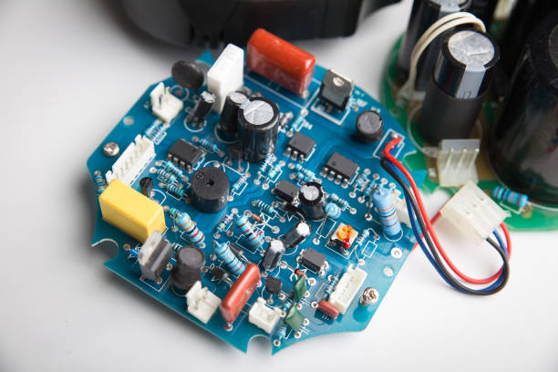
PTFE High-Frequency PCB Manufacturing
As electronic systems continue to operate at higher frequencies and data rates, PCB materials have an increasingly direct impact on signal integrity, transmission loss, impedance stability, and overall system reliability. Conventional FR-4 materials remain suitable for many electronic products, but demanding RF and microwave applications often require specialized low-loss dielectric materials.
PTFE High-Frequency PCB technology is widely considered for applications where low dielectric loss, stable electrical performance, and reliable high-frequency signal transmission are important. PTFE-based laminates can provide electrical characteristics suited to RF, microwave, wireless communication, radar, aerospace, and other high-frequency systems.
However, manufacturing PTFE PCBs is more challenging than manufacturing conventional circuit boards. PTFE’s softness, low surface energy, thermal expansion characteristics, and specialized bonding requirements require careful control throughout drilling, copper adhesion, lamination, circuit formation, and final inspection.
For this reason, successful High-Frequency PCB Manufacturing requires close coordination between material selection, PCB design, fabrication processes, and electrical performance requirements.
Key Advantages of PTFE High-Frequency PCB Materials
PTFE-based laminates offer several characteristics that make them attractive for high-frequency circuit applications.
Low Dielectric Loss and Stable Electrical Performance
One of the primary advantages of PTFE is its favorable dielectric behavior at high frequencies. Low dielectric loss can help reduce signal attenuation as electromagnetic energy travels through the transmission structure.
For RF and microwave circuits, stable dielectric properties are important because variations in dielectric characteristics can influence impedance, propagation behavior, phase performance, and signal integrity.
When combined with appropriate PCB stack-up design and controlled trace geometry, PTFE materials can support demanding high-frequency transmission requirements.
Material selection should not be based on dielectric constant alone. Engineers should also evaluate dissipation factor, frequency dependence, copper roughness, thermal characteristics, dimensional stability, and compatibility with the intended manufacturing process. GOPCBA’s technical resources also emphasize that high-frequency material selection should consider the complete electrical and manufacturing environment rather than a single material parameter.
Chemical Resistance and Environmental Stability
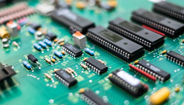
PTFE is known for strong chemical resistance and good resistance to demanding environmental conditions.
These characteristics can be valuable in specialized electronic systems where the PCB may encounter temperature fluctuations, humidity, chemicals, or other challenging operating conditions.
For aerospace, defense, industrial, and communication equipment, material stability can contribute to predictable long-term electrical performance.
However, the final reliability of a PTFE PCB depends on the complete material system and manufacturing process. Laminate construction, copper adhesion, mechanical design, surface finish, thermal cycling, and environmental protection all need to be evaluated together.
Thermal Performance
High-frequency circuits may generate heat through active components, power amplifiers, and conductor losses. Thermal design therefore remains an important consideration even when the primary objective is signal integrity.
Depending on the laminate system and PCB construction, designers may combine PTFE-based materials with other materials, metal structures, thermal vias, or mixed-material stack-ups to balance high-frequency performance with thermal management.
Challenges in PTFE High-Frequency PCB Manufacturing
Although PTFE offers excellent electrical properties for high-frequency applications, its physical characteristics create several manufacturing challenges.
Drilling and Mechanical Processing
PTFE is relatively soft compared with conventional rigid PCB materials. During drilling and routing, improper tool selection or excessive mechanical force can cause deformation, burrs, dimensional instability, or other fabrication problems.
Drilling parameters must therefore be carefully optimized according to the specific laminate construction, board thickness, hole diameter, and production requirements.
Tool condition is also important. Worn tooling can increase mechanical stress and reduce hole quality.
For multilayer PTFE boards, the manufacturer must additionally control registration and dimensional stability throughout the complete fabrication process.
Copper Adhesion
PTFE has a low surface energy, which can make copper adhesion more difficult than with conventional epoxy-based laminates.
Reliable copper adhesion is particularly important for plated-through holes, copper traces, and multilayer structures because poor bonding can negatively affect electrical and mechanical reliability.
Depending on the material system, specialized surface preparation may be required. Plasma treatment, chemical treatment, and other compatible processes can improve surface characteristics before metallization or lamination.
The exact treatment should be determined according to the selected PTFE laminate because different high-frequency materials can have different constructions and processing requirements.
Thermal Expansion and Dimensional Stability
PTFE-based materials can exhibit significant dimensional changes with temperature. This characteristic must be considered during PCB design and manufacturing.
Thermal expansion can affect:
- Layer registration
- Hole-to-pad alignment
- Trace geometry
- Multilayer dimensional stability
- Mechanical stress
- High-frequency electrical performance
For high-precision RF designs, stack-up engineering and process control are therefore essential.
GOPCBA’s high-frequency PCB manufacturing guidance highlights the importance of controlling dielectric thickness, copper roughness, trace width, layer registration, and material properties because variations in these parameters can affect impedance and signal loss.
Manufacturing Technologies for PTFE PCBs
Producing a reliable PTFE PCB requires specialized process control from material preparation through final testing.
Precision Drilling
Precision CNC drilling equipment and appropriate carbide tooling can help maintain hole accuracy while minimizing deformation.
Drilling parameters should be optimized for:
- Spindle speed
- Feed rate
- Tool geometry
- Hole diameter
- Board thickness
- Stack height
- Material construction
Unlike standard FR-4 processing, PTFE drilling may require more conservative stack-up strategies to maintain hole quality and dimensional accuracy.
After drilling, hole cleaning and surface preparation are particularly important because PTFE debris and residues can affect subsequent metallization.
Plasma and Chemical Surface Treatment
After mechanical processing, specialized surface treatment may be used to improve the condition of PTFE surfaces.
Plasma treatment can modify the surface characteristics of PTFE and improve its compatibility with subsequent metallization or bonding processes.
Chemical treatment may also be used for certain material systems.
The objective is to establish a sufficiently reliable interface between the PTFE-based dielectric and the copper structure without compromising the electrical characteristics of the laminate.
Lamination and Bonding
Multilayer PTFE PCB manufacturing requires careful control of bonding and lamination.
Temperature, pressure, heating rate, cooling rate, dielectric thickness, and material compatibility can influence the final board structure.
For mixed-material constructions, the thermal expansion characteristics of each material should also be considered. Combining PTFE with FR-4 or other laminate systems may provide cost, mechanical, or manufacturing advantages, but the stack-up must be engineered carefully to manage differences in electrical and thermal properties.
Copper Foil Selection
Copper surface roughness can become increasingly important as operating frequency rises.
At high frequencies, the skin effect concentrates current near the conductor surface. Excessive copper roughness can increase conductor loss and negatively affect high-frequency transmission.
For this reason, low-profile or ultra-low-profile copper foil may be selected for demanding RF applications.
Copper foil selection should therefore consider:
- Surface roughness
- Copper thickness
- Adhesion requirements
- Current requirements
- Frequency range
- Signal-loss targets
- Manufacturing compatibility
PTFE PCB Design Considerations
Manufacturing quality alone cannot compensate for an unsuitable high-frequency PCB design. Electrical design and fabrication engineering should be coordinated from the beginning of the project.
Controlled Impedance
Transmission-line impedance is strongly influenced by trace width, copper thickness, dielectric thickness, dielectric constant, and reference-plane configuration.
For RF and microwave circuits, the PCB manufacturer should work from a defined stack-up and impedance target.
Changes in dielectric thickness or trace geometry during manufacturing can alter the actual impedance. Therefore, process tolerances must be considered when establishing the PCB fabrication specification.
A RF PCB manufacturer should be capable of coordinating material selection, stack-up design, impedance control, and fabrication tolerances to achieve consistent electrical characteristics.
Trace Geometry and Signal Routing
High-frequency signals are more sensitive to routing geometry than conventional low-speed signals.
Designers should pay particular attention to:
- Trace width
- Trace spacing
- Reference planes
- Ground continuity
- Via transitions
- Return-current paths
- Connector transitions
- Copper surface roughness
Avoiding unnecessary discontinuities can help maintain signal integrity throughout the transmission path.
GOPCBA supports high-frequency PCB, RF PCB, controlled-impedance PCB, multilayer PCB, and Rogers mixed-lamination PCB technologies.
Layer Stack-Up
A properly engineered multilayer stack-up can provide controlled dielectric thickness, stable reference planes, and predictable impedance.
For high-frequency applications, the stack-up should be defined before routing is finalized. The selected laminate, prepreg or bonding system, copper foil, and final dielectric thickness all contribute to the electrical characteristics of the finished board.
For complex RF designs, a manufacturer should verify that the proposed stack-up can be consistently fabricated within the required tolerances.
Applications of PTFE High-Frequency PCBs
The electrical and environmental characteristics of PTFE materials make them suitable for a wide range of demanding applications.
5G and Wireless Communication
5G infrastructure requires high-frequency and high-speed signal transmission with increasingly demanding requirements for insertion loss, impedance stability, and signal integrity.
PTFE-based materials can be used in RF circuits, antenna structures, filters, amplifiers, and other high-frequency modules where low-loss electrical performance is important.
As wireless systems move toward higher frequencies, material selection becomes increasingly important. GOPCBA provides high-frequency, high-speed, multilayer, and impedance-controlled PCB manufacturing solutions for communication applications.
Satellite and Aerospace Electronics
Satellite communication and aerospace electronics operate under demanding environmental conditions and often require highly predictable RF performance.
PTFE-based PCB materials can be used in antenna systems, RF front ends, microwave circuits, satellite communication equipment, and other high-frequency electronic assemblies.
In these applications, electrical performance must be considered together with thermal cycling, mechanical stability, reliability, and manufacturing consistency.
Automotive Radar and High-Frequency Vehicle Electronics
Modern vehicles increasingly use radar and other high-frequency sensing technologies for advanced driver assistance and automated driving functions.
Radar circuits require stable RF transmission characteristics and carefully controlled impedance. PTFE and other specialized low-loss materials can be considered for radar PCB applications where conventional materials may not provide the desired high-frequency performance.
Automotive electronics also introduce additional requirements involving vibration, temperature cycling, electromagnetic compatibility, and long-term reliability. Advanced automotive PCB manufacturing therefore requires coordinated control of material selection, stack-up, impedance, thermal management, and manufacturing quality.
Radar, Defense, and Specialized RF Systems
Radar, RF communication, electronic sensing, and other specialized systems can require low-loss substrates and highly controlled electrical characteristics.
PTFE-based PCB technology can provide a suitable material platform for these demanding circuits when properly matched to the operating frequency, thermal conditions, mechanical construction, and manufacturing process.
PTFE PCB Quality Control
Because PTFE materials require specialized processing, quality control should cover both conventional PCB manufacturing parameters and high-frequency electrical characteristics.
Material Inspection
Incoming laminate should be verified against the required material specification.
Important parameters may include:
- Dielectric constant
- Dissipation factor
- Laminate thickness
- Copper thickness
- Copper surface profile
- Dimensional characteristics
- Material construction
Consistent material properties are particularly important for impedance-controlled and RF applications.
Dimensional and Visual Inspection
Inspection should verify:
- Trace width
- Trace spacing
- Hole diameter
- Hole position
- Board dimensions
- Layer registration
- Surface condition
- Copper integrity
For high-density or multilayer PTFE boards, dimensional control becomes increasingly important because small manufacturing deviations can influence electrical performance.
Electrical Testing
Electrical testing can identify open circuits, shorts, and other manufacturing defects.
For impedance-sensitive applications, additional testing or validation may be required depending on the customer’s electrical specifications.
GOPCBA’s PCB manufacturing capabilities include controlled-impedance PCB fabrication, high-frequency PCB production, multilayer PCB manufacturing, and 100% electrical testing.
Prototype Development for PTFE High-Frequency PCBs
PTFE PCB projects benefit from prototype validation before production quantities are finalized.
A prototype can be used to verify:
- Material selection
- Stack-up construction
- Controlled impedance
- RF signal performance
- Hole quality
- Mechanical dimensions
- Connector integration
- Thermal behavior
- Assembly compatibility
- Manufacturing feasibility
Early prototype validation can help identify design or process problems before they become expensive production issues.
For new RF products, prototype manufacturing can also provide an opportunity to compare different laminate systems and evaluate whether a PTFE-based material is actually necessary for the target frequency and electrical performance.
GOPCBA provides PCB prototype manufacturing services to help engineers move from initial design verification toward production while addressing manufacturability and performance requirements.
Why Choose Specialized PTFE PCB Manufacturing?
PTFE PCB manufacturing requires a combination of high-frequency material knowledge, precision fabrication, process control, and electrical engineering support.
A suitable manufacturing partner should be able to evaluate the complete project rather than treating PTFE as simply another PCB substrate.
Important capabilities include:
- High-frequency laminate processing
- PTFE material handling
- Controlled-impedance fabrication
- Precision drilling
- Specialized surface treatment
- Multilayer lamination
- Low-profile copper processing
- RF-oriented DFM review
- Electrical testing
- Prototype and production support
GOPCBA provides advanced PCB fabrication capabilities covering high-frequency PCB, RF PCB, Rogers mixed-lamination PCB, multilayer PCB, controlled-impedance PCB, HDI PCB, and other specialized circuit board technologies.
Conclusion
PTFE high-frequency PCB technology provides an important solution for electronic systems where low transmission loss, stable dielectric performance, and reliable RF signal integrity are critical.
However, the advantages of PTFE materials can only be fully realized when the PCB is designed and manufactured with appropriate processes. Drilling, copper adhesion, surface treatment, lamination, copper roughness, dimensional stability, impedance control, and electrical testing all require careful consideration.
For applications such as 5G communication, satellite systems, automotive radar, aerospace electronics, and specialized RF equipment, selecting the right PTFE material and manufacturing process can significantly influence final system performance.
The most effective approach is to evaluate material characteristics, frequency requirements, PCB structure, thermal conditions, manufacturing tolerances, and cost as one integrated engineering system. With appropriate design and controlled High-Frequency PCB Manufacturing, PTFE-based circuit boards can provide a reliable foundation for increasingly demanding high-speed and RF electronic systems.