Professional Mixed Material PCB Supplier
A Mixed Material PCB combines different substrate materials within the same circuit board to achieve specific electrical, thermal, mechanical, or high-frequency performance requirements. Because different materials can provide complementary properties, mixed material PCB technology has become increasingly important in complex electronic systems.
For demanding applications, selecting a professional supplier requires more than basic PCB fabrication capability. A qualified manufacturer should have strong material expertise, advanced lamination technology, comprehensive quality control, flexible customization capabilities, and responsive engineering support. These capabilities help ensure that mixed material circuit boards meet the increasingly diverse requirements of modern electronics.
Strong Technical Expertise and Process Development
The core challenge of a Mixed Lamination PCB is achieving compatibility and reliable integration between different substrate materials. A professional manufacturer needs a detailed understanding of the physical and chemical characteristics of high-frequency materials, high-temperature laminates, flexible materials, conventional FR-4, and other specialized substrates.
Different materials can have significantly different coefficients of thermal expansion, dielectric constants, thermal characteristics, and dimensional stability. During lamination, these differences can create mechanical stress and dimensional variation. If they are not properly controlled, problems such as delamination, blistering, warpage, and registration errors may occur.
For example, when high-frequency material is combined with conventional FR-4, the lamination temperature, pressure, heating rate, and cooling process must be carefully controlled. Managing the dimensional changes of each material is essential for maintaining layer registration and circuit geometry.
A professional PCB Manufacturing partner should therefore evaluate material compatibility during the engineering stage rather than treating material selection as a simple purchasing decision. Stack-up design, dielectric thickness, copper weight, thermal requirements, impedance targets, and lamination parameters should all be considered together.
Specialized process development is equally important. Mixed material PCBs may incorporate blind vias, buried vias, microvias, stepped structures, controlled-depth drilling, and other advanced manufacturing features. Combining these technologies requires stable process control and experienced engineering teams.
For high-density designs, precise multilayer registration is particularly important. Advanced alignment and lamination processes can help maintain accurate positioning between different substrate layers and support reliable interconnections.
Complex post-lamination machining may also be required. CNC processing and precision drilling can be used to produce stepped structures, countersunk holes, slots, and other customized mechanical features while maintaining the dimensional accuracy required for final assembly.
This technical capability is developed through continuous manufacturing experience, process optimization, equipment investment, and engineering improvement rather than through a single manufacturing step.
Comprehensive Quality Control Throughout the Manufacturing Process
The quality of a mixed material PCB directly affects the reliability and operating performance of the final electronic product. A professional supplier should therefore establish quality controls covering the entire manufacturing process, from incoming materials to final inspection.
During material preparation, each batch of laminate should be verified against the approved specifications. Important characteristics may include dielectric properties, material thickness, copper thickness, thermal performance, and compatibility with the selected lamination process.
Before lamination, surface preparation is also important. Proper cleaning removes contaminants and improves the bonding conditions between layers. For mixed material structures, surface condition and material compatibility can have a significant impact on long-term layer adhesion.
During lamination, critical process parameters such as temperature, pressure, heating rate, vacuum conditions, and cooling rate should be controlled according to the material combination and stack-up design.
Real-time process monitoring can help reduce variation and identify abnormal conditions before they result in production defects.
After fabrication, inspection should go beyond basic visual examination. Electrical continuity and insulation testing are fundamental, while advanced inspection methods can be selected according to the board’s construction and application requirements.
Cross-sectional analysis can help verify internal layer bonding, copper plating, via structures, and dielectric thickness. Impedance testing can also be used for boards containing high-speed or high-frequency circuits where transmission-line performance is critical.
For complex Multilayer PCB structures, inspection may include automated optical inspection, X-ray inspection, dimensional verification, electrical testing, and other process-specific controls.
A systematic quality management approach helps ensure that manufacturing results remain consistent across production batches and that the finished boards satisfy the customer’s technical specifications.
Flexible Customization for Different Applications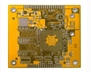
Different industries have different requirements for mixed material PCB construction. A professional supplier should therefore provide engineering-based customization rather than simply modifying standard production parameters.
For industrial control equipment operating in elevated-temperature environments, for example, a combination of high-Tg material and conventional substrate may be selected to improve thermal stability and reliability.
For medical electronics, rigid and flexible materials may be integrated to support lightweight construction and reliable electrical connections in compact or mechanically constrained spaces.
For communication and RF equipment, combining conventional materials with specialized high-frequency laminates can provide a balance between manufacturing practicality and electrical performance.
The material combination should be determined according to the actual requirements of the application. Important factors may include:
- Operating frequency
- Signal integrity
- Dielectric constant
- Dielectric loss
- Thermal requirements
- Mechanical requirements
- Layer count
- Copper thickness
- Impedance requirements
- Manufacturing volume
- Product reliability requirements
For applications requiring controlled electrical performance, High Frequency PCB technology may be integrated into a mixed-material stack-up. Material selection, trace geometry, dielectric thickness, copper roughness, and reference-plane configuration should be evaluated together to achieve predictable high-frequency performance.
The customization process should begin with engineering review. A capable supplier can evaluate the customer’s design, identify potential manufacturing risks, recommend suitable materials and stack-up structures, and optimize the manufacturing process before production begins.
This engineering-driven approach can reduce unnecessary design iterations and improve the transition from prototype development to production.
Efficient Response and Production Support
Fast response is another important characteristic of a professional mixed material PCB supplier.
The manufacturing process often begins with customer requirements, Gerber files, stack-up information, material specifications, impedance requirements, mechanical drawings, and other technical documentation. An efficient engineering workflow can quickly review these requirements and identify potential production challenges.
For prototype and low-volume projects, rapid engineering evaluation and sample production can be particularly valuable. Customers can verify electrical performance, mechanical fit, thermal behavior, and assembly compatibility before committing to larger production volumes.
An integrated manufacturer can also support a complete development process from PCB prototype to production. This can reduce the communication problems that sometimes occur when engineering, fabrication, and assembly are handled by multiple unrelated suppliers.
For advanced projects, early DFM analysis can identify issues related to trace spacing, drilling, layer registration, via structures, material selection, stack-up design, and manufacturability.
A professional supplier should also be able to adjust production resources according to project requirements. This flexibility is especially useful for engineering samples, pilot production, small batches, and products transitioning toward volume manufacturing.
Advanced Technology for Complex PCB Structures
Mixed material PCB manufacturing is often associated with complex multilayer constructions. Depending on the application, the board may incorporate different material systems, high layer counts, fine-line circuits, controlled impedance, blind vias, buried vias, microvias, and other advanced structures.
For high-density electronic products, HDI technology can provide additional routing density and compact interconnection structures. HDI PCB Manufacturing can be particularly useful when mixed-material designs also require fine-pitch component breakout or advanced via structures.
Blind and buried vias can reduce routing constraints and allow designers to create more efficient interconnections between selected layers. These technologies must be carefully coordinated with the stack-up, lamination sequence, drilling process, and material system.
For high-speed applications, unnecessary via stubs can negatively affect signal integrity. In suitable multilayer structures, controlled-depth drilling or back drilling can be used to reduce unwanted via sections. Back Drilling PCB Technology can therefore be considered as part of a broader high-speed interconnection strategy.
The selection of these technologies should always be based on electrical requirements, mechanical constraints, reliability targets, manufacturing feasibility, and overall cost.
Professional PCB Manufacturing Capabilities
A reliable supplier should have manufacturing capabilities that extend beyond basic circuit board fabrication. A comprehensive production system can support multiple PCB technologies and provide engineering assistance throughout the product development cycle.
Modern PCB Manufacturing may include:
- Single-sided and double-sided PCB fabrication
- Multilayer PCB manufacturing
- HDI PCB manufacturing
- High-frequency PCB fabrication
- High-speed PCB manufacturing
- Rigid-flex PCB production
- Heavy copper PCB manufacturing
- High-Tg PCB manufacturing
- Blind and buried via technology
- Controlled-impedance PCB manufacturing
- Prototype and low-volume production
An integrated PCB Manufacturing Service can help customers manage different PCB technologies through a single manufacturing partner.
For development projects, prototype production is also an important part of the supplier’s capabilities. A PCB Prototype Manufacturing Service allows engineers to validate the mixed-material stack-up, electrical characteristics, mechanical dimensions, and assembly performance before production is scaled.
This continuity from prototype to production can help minimize manufacturing transfer risks and maintain process consistency.
Technical Support Beyond Product Delivery
A professional supplier’s responsibilities should not end when the circuit boards are shipped. Long-term technical support can help customers achieve more reliable product performance throughout the PCB lifecycle.
Customers may require guidance on storage conditions, moisture management, soldering temperatures, assembly processes, thermal exposure, and other handling requirements.
Mixed material structures can have specific processing considerations because different substrates may respond differently to thermal cycles. Providing appropriate manufacturing and assembly recommendations can help customers avoid unnecessary reliability problems.
When issues arise during equipment testing or product assembly, an experienced technical team should be able to investigate whether the problem is related to PCB material selection, lamination, electrical performance, dimensional accuracy, assembly conditions, or other factors.
For complex projects, technical cooperation can begin during the early design stage. Engineers and PCB manufacturers can work together to optimize material combinations, stack-up structures, routing requirements, impedance targets, and manufacturing processes.
This collaborative approach transforms the supplier from a simple PCB producer into a long-term engineering partner.
How to Choose a Professional Mixed Material PCB Supplier
Selecting the right supplier requires evaluating technical capability, quality systems, manufacturing experience, customization flexibility, and engineering support together.
Key factors to consider include:
- Experience with mixed-material stack-ups
- Material compatibility analysis
- Advanced lamination capabilities
- Multilayer registration control
- High-frequency material processing
- HDI and microvia technology
- Controlled-impedance manufacturing
- Back drilling capability
- Electrical and dimensional testing
- Prototype and low-volume production
- DFM engineering support
- Production scalability
- Responsive technical service
A supplier with broad manufacturing capabilities can provide a more practical solution when project requirements change during development.
For example, a design may initially require a conventional multilayer structure but later need high-frequency materials, HDI technology, controlled impedance, or back drilling as electrical requirements become more demanding. Working with a manufacturer capable of supporting these technologies can simplify the development process.
Conclusion
The value of a professional mixed material PCB supplier lies in the combination of technology, quality, customization, and service.
Successful mixed-material PCB production requires much more than combining different laminates in one board. Material compatibility, thermal expansion, dielectric properties, lamination parameters, layer registration, via structures, impedance requirements, and manufacturing tolerances must all be considered as part of an integrated engineering process.
A capable supplier should provide comprehensive Mixed Material PCB solutions from engineering evaluation and material selection through fabrication, inspection, prototype development, and production support.
As electronic products continue to become smaller, faster, and more complex, mixed-material PCB technology will play an increasingly important role in high-frequency communication, industrial control, medical electronics, automotive systems, networking equipment, and other advanced applications.
Choosing a supplier with strong engineering capabilities, stable manufacturing processes, rigorous quality control, and flexible customization support can help customers achieve reliable PCB performance while reducing development and production risks.