0.15mm Mechanical Blind and Buried Via PCB
As electronic devices continue becoming smaller, thinner, and more powerful, PCB routing density has become one of the major limitations affecting system performance. The 0.15mm Blind Via PCB technology provides an advanced interconnection solution for high-density multilayer circuit boards by creating compact layer-to-layer connections.
Compared with traditional through-hole structures, blind and buried vias reduce occupied routing space, improve design flexibility, shorten signal paths, and support lower-loss signal transmission. This technology has become an essential foundation for advanced electronic products requiring high integration density, including mobile devices, industrial controllers, medical systems, automotive electronics, and high-frequency communication equipment.
A well-designed HDI PCB structure using small-diameter blind and buried vias enables engineers to achieve greater component density while maintaining electrical reliability and signal performance.
Core Characteristics of 0.15mm Mechanical Blind and Buried Via PCB
High Via Diameter Accuracy and Consistency
A 0.15mm mechanical blind and buried via is not simply a smaller hole. It requires highly precise drilling technology capable of maintaining strict dimensional control throughout multilayer PCB manufacturing.
The typical via diameter tolerance can be controlled within ±0.01mm, ensuring reliable contact between the drilled hole wall and copper plating layer.
High dimensional accuracy prevents instability caused by excessive hole variation and ensures consistent electrical performance during mass production.
For advanced multilayer circuit structures, precise via control must work together with stack-up design, material selection, and layer alignment. Learn more about Multilayer PCB Manufacturing and advanced multilayer fabrication methods.
Superior Hole Wall Quality
Mechanical drilling equipment designed for high-density PCB production can achieve smooth hole walls with minimal defects.
High-quality blind and buried vias require:
- Low hole-wall roughness
- No burr formation
- Uniform copper plating coverage
- Stable electrical performance
A smooth hole wall reduces signal reflection and transmission loss, especially in high-frequency applications.
Compared with conventional through-hole structures, optimized blind and buried via designs can significantly improve signal performance by shortening electrical paths and reducing unnecessary discontinuities.
Uniform copper thickness inside the via also improves current conduction reliability and prevents localized overheating during operation.
Precise Depth Control
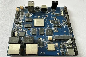
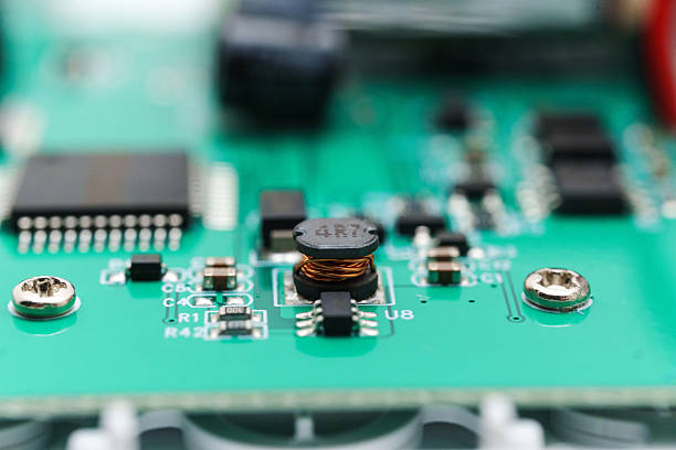
Blind via depth accuracy is critical because it directly affects layer-to-layer connection reliability.
For example, in a six-layer PCB, a blind via connecting the outer layer to an internal layer must stop precisely at the target layer. Excessive drilling depth may damage internal circuits, while insufficient depth may result in poor electrical connection.
Advanced mechanical blind via processing can achieve depth control within tight tolerances, improving space utilization and allowing more flexible routing strategies.
By optimizing via depth and layer configuration, designers can significantly increase PCB routing density while maintaining reliable electrical performance.
Broad Material Compatibility
The 0.15mm mechanical blind and buried via process can support various PCB materials, including standard FR-4 laminates and high-frequency materials.
Different materials require optimized drilling parameters such as:
- Spindle speed
- Feed rate
- Tool geometry
- Cooling conditions
- Material thickness compensation
Through process optimization, manufacturers can achieve stable via formation across different PCB thickness ranges.
For applications requiring high-frequency performance and low signal loss, advanced materials and controlled stack-up designs are often combined with blind and buried via technology. More information is available in High Frequency PCB Manufacturing.
Advanced Manufacturing Processes
Sequential Drilling Technology
Blind and buried via fabrication often uses sequential processing rather than a single drilling operation.
A typical manufacturing approach includes:
- Drilling blind vias on individual layers
- Performing copper plating
- Laminating multiple PCB layers together
- Creating buried vias through additional processing
This step-by-step process improves layer alignment accuracy and reduces the risk of via position deviation.
Sequential fabrication is especially important for complex HDI PCB structures where multiple interconnection levels must be accurately integrated.
Advanced Copper Plating Technology
Reliable copper plating is essential for small-diameter vias.
Because the via opening is extremely small, copper ions must be deposited evenly throughout the hole wall. Advanced plating processes improve copper distribution and prevent defects such as uneven thickness or incomplete filling.
Key control factors include:
- Current density
- Chemical concentration
- Solution circulation
- Plating time
- Temperature control
A uniform copper layer improves electrical conductivity and mechanical strength, ensuring stable connections during long-term operation.
For high-density interconnection technologies, see HDI PCB Manufacturing Technology.
Laser Positioning and Mechanical Drilling Combination
A hybrid process combining laser positioning and mechanical drilling can further improve via accuracy.
The process typically involves:
- Creating a precision positioning hole using laser technology
- Expanding the hole to the required diameter using mechanical drilling
This method improves drilling alignment and supports high-density component areas such as BGA packages.
Accurate positioning is especially important when thousands of micro connections must be created within a limited PCB area.
Thermal Reliability Testing
Blind and buried via PCBs must undergo strict reliability verification to ensure long-term performance.
Common reliability evaluations include:
- Thermal cycling tests
- Temperature shock testing
- High-humidity pressure testing
- Cross-sectional analysis
These tests verify:
- Via wall integrity
- Copper adhesion strength
- Layer bonding reliability
- Resistance to environmental stress
Reliable testing ensures that the PCB can maintain stable electrical connections under demanding operating conditions.
Applications of 0.15mm Mechanical Blind and Buried Via PCB
Smartphone Mainboards
Modern smartphones require extremely high component density within a very limited physical space.
The High Density PCB structure enabled by 0.15mm blind and buried vias allows designers to place advanced processors, memory devices, RF modules, and power management circuits in compact layouts.
In foldable smartphones and flagship devices, high-density via technology helps increase connection points while reducing PCB size.
The shorter electrical paths also improve signal performance for high-speed interfaces and advanced communication functions.
Industrial Robot Controllers
Industrial robots require complex control systems capable of processing multiple sensor signals, motor controls, and communication interfaces simultaneously.
A blind and buried via PCB allows engineers to separate:
- Analog signal layers
- Digital signal layers
- Power distribution layers
- Ground reference structures
This improves electromagnetic compatibility and reduces interference between different functional circuits.
In multi-axis robotic systems, high-density PCB technology supports compact controller designs while maintaining reliable operation in industrial environments.
Medical Ultrasound Equipment
Medical ultrasound systems require accurate transmission and processing of multiple sensitive signals.
The compact interconnection capability of a Buried Via PCB allows designers to create independent signal paths with improved shielding and noise control.
In ultrasound probe electronics, advanced PCB structures help maintain signal accuracy and improve image quality by reducing unwanted interference.
Medical equipment applications require especially high reliability because signal errors may directly affect diagnostic performance.
Automotive Radar Modules
Automotive millimeter-wave radar systems require high-frequency signal processing and dense RF routing.
Traditional via structures may introduce unnecessary signal path length and additional parasitic effects. Blind and buried via technology helps shorten critical RF connections and reduce insertion loss.
For radar and high-frequency automotive electronics, controlled impedance design is also essential. More details can be found in PCB Impedance Control Design.
Future Development of Blind and Buried Via Technology
The value of 0.15mm mechanical blind and buried via technology lies in solving the fundamental challenges of modern electronics: higher density, smaller size, faster transmission, and greater reliability.
As technologies such as advanced packaging, chiplet architectures, and high-performance computing continue developing, smaller and more precise interconnection structures will become increasingly important.
Future HDI PCB solutions will continue moving toward:
- Smaller via dimensions
- Higher layer integration
- Lower signal loss
- Improved thermal performance
- Greater manufacturing precision
Through continuous improvements in materials, drilling technology, plating processes, and design optimization, blind and buried via PCBs will remain a critical technology supporting next-generation electronic systems.