How to Use a PCB Board in an Electronics Project: PCB Design, Manufacturing & Assembly Guide
Printed circuit boards (PCBs) are the backbone of modern electronics. From small remote-controlled cars and household appliances to advanced flight control systems, medical equipment, and industrial devices, PCBs are found in almost every electronic product.
For students, engineers, and electronics hobbyists, a breadboard is often the first place where an idea becomes a working circuit. Breadboards are excellent for prototyping because components can be inserted, removed, and rearranged without soldering. However, as a circuit becomes more complex, the number of jumper wires can quickly make the prototype difficult to build, troubleshoot, and maintain.
Once a circuit has been successfully tested on a breadboard, the next logical step is often to transfer the design to a PCB. A properly designed PCB provides permanent electrical connections, better mechanical stability, improved reliability, and a much cleaner product design.
So, how do you use a PCB board in an electronics project? The basic process involves designing the circuit, creating the PCB layout, selecting the appropriate PCB type and materials, manufacturing the board, assembling the components, and finally testing the completed circuit.
This guide explains each step and provides practical recommendations for using a PCB board effectively in an electronics project.
What Is a PCB?
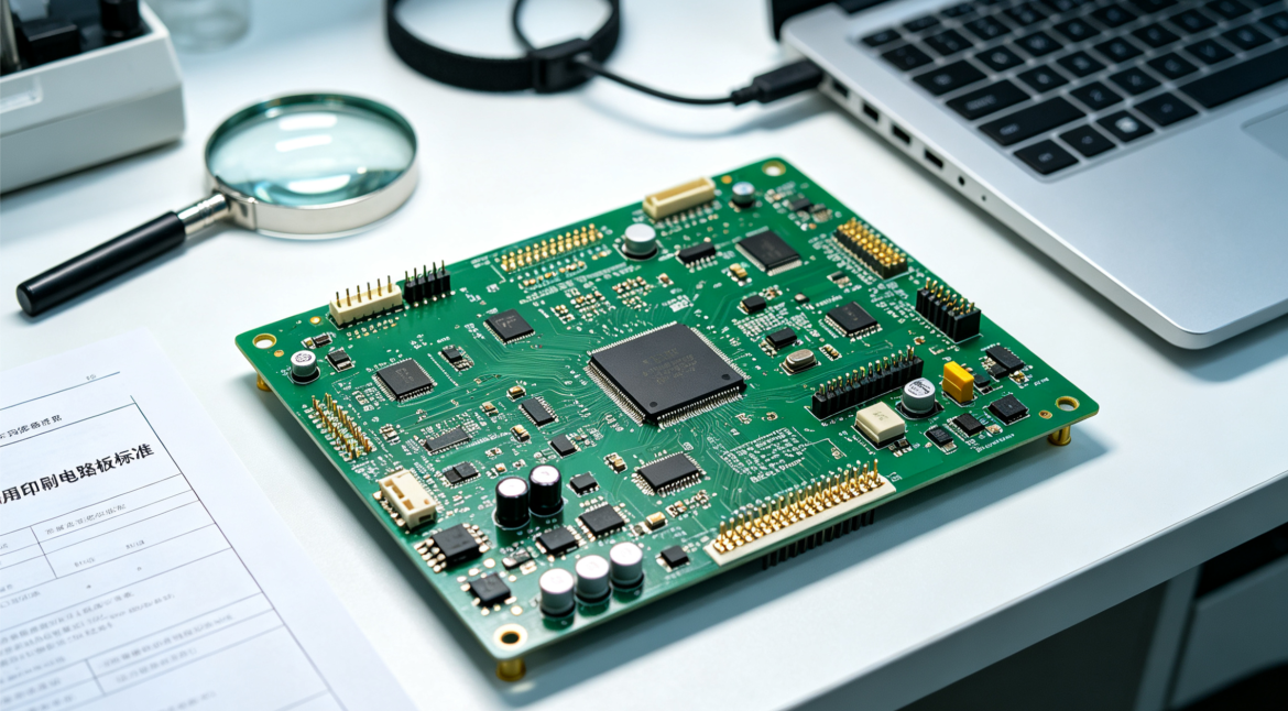
A printed circuit board (PCB) is a flat board made from an insulating substrate with conductive copper layers used to electrically and mechanically connect electronic components.
Unlike a breadboard, which relies on temporary jumper wires and plug-in connections, a PCB uses copper traces, pads, vias, and other conductive structures to create permanent electrical connections between components.
A typical PCB may contain:
- Copper traces for electrical connections
- Component pads for soldering
- Vias for connecting different PCB layers
- Solder mask for protecting exposed copper
- Silkscreen for component labels and reference designators
- Ground and power planes
- Mounting holes for mechanical installation
This structure makes a PCB board more compact, reliable, and suitable for permanent electronic products.
For simple projects, a single-layer PCB may be sufficient. More complex designs may require two-layer or multilayer PCBs to provide enough routing space, power distribution, grounding, and signal integrity.
How to Prepare a PCB for an Electronics Project
Once a circuit has been successfully tested on a breadboard, you can begin preparing the PCB version of the design.
The process typically involves five major stages:
- Circuit schematic design
- PCB layout planning
- PCB type and material selection
- PCB manufacturing
- PCB assembly and testing
Each stage affects the performance, reliability, cost, and manufacturability of the final electronic product.
1. Design the Electronic Circuit
The first step in PCB Design is creating a schematic that represents the electrical connections between components.
ECAD software such as KiCad, EasyEDA, and Altium Designer can be used to create the schematic. These tools allow engineers and hobbyists to define components, electrical connections, power networks, and design rules before converting the schematic into a physical PCB layout.
A well-prepared schematic should include:
- Microcontrollers and ICs
- Resistors and capacitors
- Diodes and transistors
- Connectors
- Power supplies and regulators
- Sensors and communication interfaces
- Ground and power connections
Before starting the PCB layout, carefully review the schematic and verify that all electrical connections are correct.
For more complex designs, circuit simulation can also help identify potential problems before the PCB is manufactured.
2. Plan the PCB Layout
After completing the schematic, the next step is to convert it into a physical PCB layout.
PCB layout determines where components are placed and how electrical connections are routed between them. Good layout planning is essential because a PCB that works correctly in theory may still experience noise, thermal, signal integrity, or manufacturing problems if the physical layout is poorly designed.
Place Components Carefully
Place components according to their electrical function, mechanical requirements, and thermal characteristics.
For example:
- Keep related components close together.
- Place connectors near the edge of the PCB.
- Keep decoupling capacitors close to IC power pins.
- Separate sensitive analog circuits from noisy switching circuits.
- Keep high-current paths short and wide.
- Provide adequate spacing around components that generate heat.
Component placement is one of the most important parts of PCB Design because it directly affects routing efficiency, assembly, troubleshooting, and overall reliability.
Use Short and Direct Traces
Whenever possible, use short and direct copper traces between electrically related components.
Power and high-current traces should generally be wider than low-current signal traces. The appropriate trace width depends on current, copper thickness, temperature rise, and other design requirements.
For high-speed or RF circuits, trace length, impedance, spacing, return paths, and layer structure become even more important.
Use Ground Planes for Complex Circuits
For more complex electronic projects, a dedicated ground plane can provide a lower-impedance return path and help reduce noise.
A multilayer PCB can use an entire internal layer as a ground plane while other layers are used for signal and power routing. Vias can connect component grounds to the appropriate plane.
However, the correct grounding strategy depends on the circuit architecture. Analog, digital, power, and RF circuits may require different grounding and return-current considerations.
Consider Thermal Management
Power components such as MOSFETs, voltage regulators, drivers, and power ICs may generate significant heat.
When designing the PCB, consider:
- Copper area
- Thermal vias
- Heatsink clearance
- Component spacing
- Airflow
- Heat dissipation paths
Adequate thermal management helps prevent excessive temperature rise and improves long-term PCB reliability.
3. Choose the Right PCB Type
A PCB can contain one or multiple conductive layers depending on the complexity and requirements of the project.
Single-Layer PCB
A single-layer PCB has copper routing on one side. It is simple, inexpensive, and suitable for basic circuits.
Typical applications include:
- Simple hobby projects
- Basic power circuits
- LED boards
- Simple control circuits
Double-Layer PCB
A double-layer PCB has copper layers on both sides and provides significantly more routing flexibility than a single-layer board.
It is commonly used for:
- Embedded systems
- Microcontroller projects
- Consumer electronics
- Industrial control boards
Multilayer PCB
A multilayer PCB contains three or more conductive layers separated by insulating materials.
Multilayer boards are useful when a project requires:
- High component density
- Complex routing
- Dedicated power planes
- Dedicated ground planes
- High-speed signal routing
- Improved electromagnetic compatibility
Flexible and Rigid-Flex PCBs
A flexible PCB can bend and conform to the mechanical structure of a product. It is useful for compact electronics, wearable devices, displays, cameras, and other applications where space or movement is important.
A rigid-flex PCB combines rigid sections with flexible sections to provide both mechanical support and flexible interconnection.
Metal-Core and Aluminum PCBs
For applications with significant heat-generation requirements, aluminum or other metal-core PCB technologies can provide improved thermal performance compared with conventional FR-4 constructions.
They are frequently considered for LED lighting, power electronics, automotive electronics, and other thermally demanding applications.
The appropriate PCB type should be selected according to electrical requirements, mechanical constraints, thermal conditions, production volume, and budget.
4. Prepare the PCB Manufacturing Files
After completing the PCB layout, run design rule checks (DRC) and verify the board carefully before manufacturing.
Typical manufacturing data may include:
- Gerber files
- NC drill files
- Board outline
- Copper layer data
- Solder mask data
- Silkscreen data
- Fabrication drawings
- Bill of materials when assembly is required
These files are used by the manufacturer to produce the physical circuit board.
Professional PCB Manufacturing typically includes processes such as imaging, etching, drilling, plating, lamination for multilayer boards, solder mask application, surface finishing, inspection, and electrical testing.
For hobby projects, a DIY PCB can also be produced using methods such as toner transfer and chemical etching. However, professionally manufactured PCBs generally provide better dimensional accuracy, repeatability, reliability, and access to advanced PCB structures.
5. Gather the Components
Once the PCB has been manufactured, the next step is to collect all required components.
Your ECAD software can typically generate a Bill of Materials (BOM) containing information such as:
- Reference designator
- Component value
- Part number
- Package type
- Manufacturer
- Required quantity
Review the BOM carefully before assembly.
It is also important to verify component specifications and package dimensions. A component with the correct electrical value may still be unsuitable if its package, voltage rating, current rating, tolerance, or temperature rating does not match the design.
6. Place Components on the PCB
After collecting the components, place them on the PCB according to the board’s silkscreen markings and assembly documentation.
For manual assembly, a practical approach is to install smaller, lower-profile components first and larger components afterward.
A typical sequence is:
- Small resistors and capacitors
- Diodes and small semiconductor devices
- ICs and other low-profile components
- Larger capacitors and inductors
- Connectors
- Switches, relays, and mechanical components
Before soldering, check the orientation of polarized components such as:
- Diodes
- LEDs
- Electrolytic capacitors
- ICs
- Transistors
- Connectors with defined orientation
Incorrect component orientation can prevent the circuit from operating or, in some cases, cause component damage when power is applied.
7. Solder the Components
PCB Assembly is the process of attaching electronic components to the circuit board and creating reliable solder joints.
For small prototypes, components can be soldered manually using a soldering iron and suitable solder wire.
For larger production volumes, manufacturers commonly use processes such as:
- Solder paste printing
- Pick-and-place assembly
- Reflow soldering
- Wave soldering
- Selective soldering
- Automated optical inspection (AOI)
For manual soldering, use an appropriately sized soldering tip and suitable solder. Avoid applying excessive heat for extended periods, particularly to temperature-sensitive components.
A good solder joint should provide a reliable mechanical and electrical connection without creating unintended bridges between adjacent pads.
8. Inspect and Test the PCB
After PCB Assembly, carefully inspect the board before applying power.
Check for:
- Missing components
- Incorrect component values
- Incorrect polarity
- Poor solder joints
- Solder bridges
- Damaged components
- Lifted pads
- Broken traces
- Contamination
- Incorrect connectors
A magnifying glass or microscope can be useful for inspecting small components and fine-pitch solder joints.
Use a Multimeter
A digital multimeter is one of the most useful tools for prototype PCB testing.
With the board unpowered, you can use resistance and continuity measurements to identify unexpected connections or possible short circuits.
With power applied, carefully measure important voltage rails and compare them with the expected values from the schematic or component datasheets.
Remember that a continuity beep does not automatically indicate a fault. Some low-resistance connections are intentional, and in-circuit measurements can be affected by other components connected in parallel.
Power the PCB Safely
When powering a newly assembled PCB for the first time, use an appropriate current-limited bench power supply whenever possible.
Start by verifying:
- Input voltage
- Polarity
- Ground connections
- Expected current consumption
- Power-rail voltages
- Regulator outputs
If the board draws unexpectedly high current, disconnect power and investigate before continuing.
9. Integrate the PCB Into the Final Project
Once the PCB passes electrical and functional testing, it can be integrated into the final electronic product.
Depending on the application, this may involve:
- Mounting the PCB inside an enclosure
- Connecting batteries or power supplies
- Installing switches and connectors
- Connecting sensors
- Attaching displays
- Connecting motors or actuators
- Securing cables
- Providing thermal management
Mechanical integration should be considered during the initial PCB Design process rather than after the board has already been manufactured.
Verify mounting-hole locations, board dimensions, connector positions, component height, cable clearance, and enclosure tolerances before final assembly.
PCB Board vs. Breadboard
A breadboard and PCB serve different purposes during electronic product development.
| Feature | Breadboard | PCB |
|---|---|---|
| Prototyping speed | Very fast | Requires design and fabrication |
| Wiring | Jumper wires | Copper traces |
| Reliability | Suitable for prototypes | Better for permanent products |
| Mechanical stability | Relatively low | High |
| Circuit density | Limited | Much higher |
| Customization | Limited | Extensive |
| High-speed performance | Often limited | Better controlled |
| Professional production | Not suitable | Suitable |
| Repeatability | Low | High |
A breadboard is excellent for quickly testing an idea, while a PCB board is generally the better choice when the circuit needs to become compact, reliable, repeatable, and suitable for integration into a finished product.
Common Mistakes When Using a PCB in an Electronics Project
Even simple PCB projects can fail because of small design or assembly mistakes.
Incorrect Component Orientation
Always check polarity and pin orientation before soldering.
Insufficient Trace Width
Power and high-current traces that are too narrow can result in excessive temperature rise or voltage drop.
Poor Grounding
Inadequate ground design can increase noise and create unexpected circuit behavior, particularly in high-speed, analog, and RF applications.
Poor Thermal Design
Power components without sufficient copper area or thermal paths can operate at excessive temperatures.
Skipping Electrical Checks
Applying power immediately after assembly without checking for shorts, incorrect polarity, or missing components increases the risk of damage.
Ignoring Mechanical Requirements
A PCB may function electrically but still fail to fit inside the enclosure because of incorrect dimensions, connector placement, or component height.
Best Practices for Using a PCB Board
To achieve reliable results, consider the following PCB Design and assembly practices:
- Test the circuit thoroughly on a breadboard before creating the PCB when appropriate.
- Review the schematic before beginning layout.
- Run DRC before generating manufacturing files.
- Use appropriate trace widths for signal and power circuits.
- Keep sensitive signal paths away from noisy power circuits.
- Provide appropriate grounding and return paths.
- Place decoupling capacitors close to IC power pins.
- Consider thermal management for high-power components.
- Verify component footprints against datasheets.
- Check component polarity before soldering.
- Inspect the board before applying power.
- Use current-limited power during initial testing.
- Perform functional testing after assembly.
- Consider DFM requirements before submitting the design for PCB Manufacturing.
Following these practices can reduce redesigns, manufacturing problems, assembly defects, and troubleshooting time.
How Kingda Can Support Your PCB Project
For projects that need to move beyond breadboard prototyping, working with an experienced PCB partner can simplify the transition from schematic to finished circuit board.
Kingda can be considered for PCB-related requirements such as PCB Design, PCB Manufacturing, and PCB Assembly, depending on the project’s technical and production requirements.
When selecting a PCB manufacturing partner, consider factors such as:
- PCB technology and layer capability
- Material options
- Board size and thickness
- Copper thickness
- Surface finish
- Manufacturing tolerances
- Quality control
- Electrical testing
- Assembly capability
- Production volume
- Lead time
- Engineering support
Choosing the right manufacturing partner early in the development process can help reduce manufacturing risks and improve the transition from prototype to production.
Frequently Asked Questions About Using a PCB Board
How do you use a PCB board in an electronics project?
To use a PCB board in an electronics project, first design and verify the circuit schematic, create the PCB layout, select the appropriate PCB type and material, generate manufacturing files, fabricate the board, assemble the components, and test the completed circuit before integrating it into the final product.
What is the difference between a breadboard and a PCB?
A breadboard is primarily used for temporary prototyping and relies on plug-in connections and jumper wires. A PCB uses permanent copper traces and soldered components, making it more compact, mechanically stable, reliable, and suitable for finished electronic products.
How do I convert a breadboard circuit to a PCB?
Start by documenting the tested breadboard circuit and creating an accurate schematic. Then select component footprints, arrange the components, route the PCB traces, run design rule checks, generate manufacturing files, and manufacture the board. After assembly, inspect and test the PCB before using it in the final project.
What PCB type should I use for my project?
The appropriate PCB type depends on circuit complexity, available space, electrical requirements, thermal conditions, mechanical constraints, and production volume. Simple circuits may use single-layer or double-layer PCBs, while complex high-density designs may require multilayer PCBs. Flexible or metal-core PCBs may be appropriate for specialized applications.
Can I make a PCB at home?
Yes. Hobbyists can manufacture simple PCBs at home using methods such as toner transfer and chemical etching. However, professional PCB Manufacturing is generally preferable for complex designs, multilayer boards, fine-pitch components, controlled impedance, high reliability, and production quantities.
How do I test a PCB before powering it on?
With the power disconnected, inspect the PCB for incorrect components, solder bridges, damaged traces, and polarity errors. Use a multimeter to check for unexpected shorts and verify important connections. When powering the board for the first time, a current-limited bench supply can provide additional protection.
Why is PCB layout important?
PCB layout determines how components and electrical connections are physically arranged. A good layout improves signal integrity, power distribution, thermal performance, manufacturability, assembly, and reliability while reducing the risk of electrical interference and design errors.
What tools are needed to build a PCB project?
Basic PCB projects typically require ECAD software, a soldering iron, solder, flux, wire cutters, tweezers, a multimeter, and inspection tools. More advanced projects may require an oscilloscope, logic analyzer, LCR meter, thermal camera, or automated PCB testing equipment.
Conclusion
A printed circuit board (PCB) provides a practical way to transform a tested electronic concept into a compact, reliable, and professional product.
The process begins with circuit schematic design and continues through PCB layout, component selection, PCB type selection, manufacturing, assembly, inspection, and functional testing. Each stage plays an important role in determining the final performance and reliability of the electronic product.
For students and hobbyists, learning how to use a PCB board in an electronics project is an important step beyond breadboard prototyping. For professional engineers, careful PCB Design, PCB Manufacturing, and PCB Assembly practices can reduce development risks and create products that are easier to manufacture, test, maintain, and scale.
Whether you are building a simple hobby circuit or developing a sophisticated electronic product, a well-designed PCB can provide the foundation needed to turn an idea into a reliable real-world device.