BMS PCB Requirements for EV Battery Management Systems
A battery management system sits between the cells and the rest of the vehicle. It measures cell voltage, pack current and temperature, then decides how the pack may charge or discharge. Every one of those decisions depends on a board that holds its accuracy over years of heat, vibration and electrical noise. The PCB is therefore not a passive carrier. It sets the measurement floor, the thermal path and the noise budget for the whole system.
This review covers the requirements that shape a BMS board and the checks that prove them. It looks at material choice, stackup, layout discipline, thermal design and test coverage. Each section explains what the decision costs and what a buyer should verify before release. The same logic applies to any high-reliability control board, but the numbers here are specific to battery management in electric vehicles.
Cell Measurement Accuracy
Cell voltage is the input that drives balancing and protection. A small error at the sense point can push a cell outside its safe window without anyone noticing. The board must carry that signal from the cell tap to the monitor IC with minimal loss and minimal pickup. Trace resistance, connector contact resistance and thermal EMF all add to the error budget. Designers should treat the sense path as a precision circuit, not as ordinary wiring.
Layout does most of the work here. Differential pairs from the tap connector to the monitor IC help reject common-mode noise. Kelvin connections at shunt resistors keep high current paths out of the measurement loop. Grounding should follow the IC vendor reference design, with a quiet analog ground kept apart from switching currents. A careful engineer will review these details during PCB design and layout, because fixing them after fabrication is expensive.
Stackup Choices
A BMS board usually carries mixed signals. High-current paths, switching converters, precision analog front ends and communication buses share one substrate. A multilayer stackup separates them by function and gives every signal a defined return path. Four layers is a common starting point, and six or eight layers appear when isolation, routing density or thermal spreading demand more copper. The stackup should be fixed before layout begins.
Plane integrity matters more than layer count. A split ground plane under a precision analog trace forces return current to detour, and that detour creates noise. Power planes should be continuous under the components they feed. Isolated domains, such as the pack-side measurement and the vehicle-side communication, need clear separation with adequate creepage and clearance. Buyers should ask for the stackup drawing and confirm that the isolation barrier is defined before tooling starts.
Thermal Path Design
Power components in a BMS generate heat in a small area. Precharge resistors, shunt paths, DC-DC converters and protection FETs all dissipate energy. Heat that cannot leave the board raises the local temperature of nearby sensors and reference circuits. That drift shows up as measurement error, so thermal design is also an accuracy issue. Copper area, thermal vias and exposed pads are the main tools available to the designer.
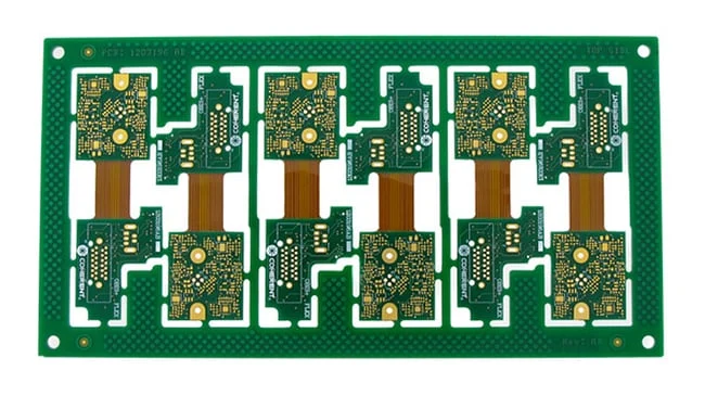
A practical approach is to plan the heat path from the first layout pass. Thermal vias under exposed pads carry heat to inner copper and to the enclosure. Thick copper on power layers spreads it further. The board outline and mounting points should be chosen so the hottest parts sit away from temperature sensors. When these decisions are made early, the board needs fewer corrections later in PCB assembly and test.
Isolation And Creepage
Electric vehicle packs operate at voltages that require solid isolation between the high-voltage domain and the low-voltage electronics. The PCB must maintain that barrier through coating, contamination and thermal cycling. Creepage and clearance distances depend on the working voltage, the pollution degree and the material group. These are design inputs, not guesses. The engineer should confirm them with the system safety plan before layout.
Slots and cutouts can extend the creepage path where space is tight. Conformal coating helps, but it cannot rescue a layout that starts with insufficient spacing. The barrier should be visible on the fabrication drawing so the board shop can inspect it. Buyers should check that the isolation area is marked, that no copper crosses it, and that the assembly process keeps coating out of connector contacts. A clear drawing prevents a costly misunderstanding.
Noise And EMC Control
A vehicle is a noisy environment. Motors, inverters, contactors and wireless modules all radiate energy, and the BMS must keep measuring through it. The board also generates its own noise from switching converters and digital clocks. Good EMC starts with a quiet layout. Sensitive traces stay short, keep a continuous return path, and avoid running beside switching nodes. Filters belong close to the connector, not in the middle of the board.
Shielding, ferrites and transient protection all help, but they work best when the layout is already disciplined. Communication lines such as CAN should be routed as pairs with controlled impedance. The stackup and trace geometry should be agreed with the fabricator so the impedance is repeatable. Buyers should ask for the impedance report and confirm that the test coupon matches the production panel. This is a routine request, and a supplier should answer it without hesitation.
Fabrication And Assembly Checks
Once the design is fixed, the board shop controls what the engineer receives. Copper weight, dielectric thickness, hole quality and surface finish all affect reliability. Heavy copper on power layers needs careful etching control. Small vias need reliable plating through the barrel. Surface finish choice affects solderability and long-term contact resistance. These are process decisions, and they should be recorded on the fabrication drawing rather than left to default.
Assembly adds its own risks. Fine-pitch monitor ICs, connectors and shunt resistors need accurate placement and a stable reflow profile. Solder joints under thermal cycling are the usual failure point, so voiding and fillet shape deserve attention. A supplier with structured SMT PCB assembly controls will inspect these features and keep the data. Buyers should ask which inspection steps run on the line and what happens when a limit is exceeded.
Test Coverage And Records
Electrical test confirms that the board works, but it also proves that the process is under control. In-circuit test checks component presence and value. Functional test verifies the measurement chain against a known reference. Boundary scan helps where dense connectors limit probe access. The test plan should be written alongside the design, because access for probes and fixtures is a layout decision.
Records turn a test result into useful evidence. A batch record should show which program ran, which fixtures were used and what the readings were. When a field return arrives, that record shortens the investigation. Buyers should ask for the test report with the shipment and confirm that the limits match the drawing. A supplier that treats PCBA testing as a data source rather than a pass or fail gate will catch drift before it becomes scrap.
Supplier And Sourcing Decisions
BMS boards often use long-life parts that are hard to second-source. The supplier should confirm availability before the build and propose approved alternates where risk exists. Counterfeit avoidance matters more here than on consumer boards, because a wrong monitor IC can defeat the whole safety concept. Traceability from reel to board is a reasonable requirement. Buyers should ask how the supplier records lot and date code information.
A partner that handles fabrication, sourcing and assembly under one scope reduces the number of handoffs where information is lost. That is the practical argument for turnkey PCB assembly on automotive projects. The engineering review, the material plan and the test plan stay with one team. Buyers still need to verify the details, but the coordination burden is lower. Ask for the DFM report, the stackup and the test plan before approving the first article.
The final check is repeatability. A good first article proves the process once, and a good record proves it again on the next order. Confirm that the drawing, the process sheet and the inspection plan agree. Then confirm that the same documents govern the repeat build. That discipline is what keeps a battery management board trustworthy over the life of the vehicle.